|
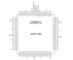
Altera MAX 7000S
- MTXPlus+ Test Bed

|
Dave's Max 7000 Development
Board
|
Hardware Test Bed
Rather than trying to go straight to
development of the glue logic for MTXPlus, I think it is a
better idea to experiment by developing some test programs
that will execute on a simple hardware test device.
Altera produce a
range of "Development" boards, including the DE1 that I use
to run a copy of Andy Key's REMEMOTECH (an emulation of the
Memotech MTX computer running on a Cyclone II FPGA (for
details on the Cyclone II, see this page on the
Altera website), as well as CPLD development boards.
These boards come in a range of prices, but a cheaper option
is to build my own test bed, which will require a bit more
effort but should be able to facilitate testing of logic
designs on real hardware.
To be able to exercise the programmed logic
and display the resultant outputs, a board with basic inputs
and outputs from switches and LEDs will do the job. Here is
my design for Dave's Development System . . . . .
[When I was half way through wiring up my
board, I discovered that Altera had produced EPM7128S based
Development boards for its
University Program - the UP1 and UP2. These boards have
two CPLDs installed, a MAX7128S and the more powerful
FLEX10K20 which has 20,000 gates. As it turns out, these
boards have remarkably similar I/O functions as my board.]
Basic Features :
-
A single board containing and EPM7128S CPLD
with input and output hardware
-
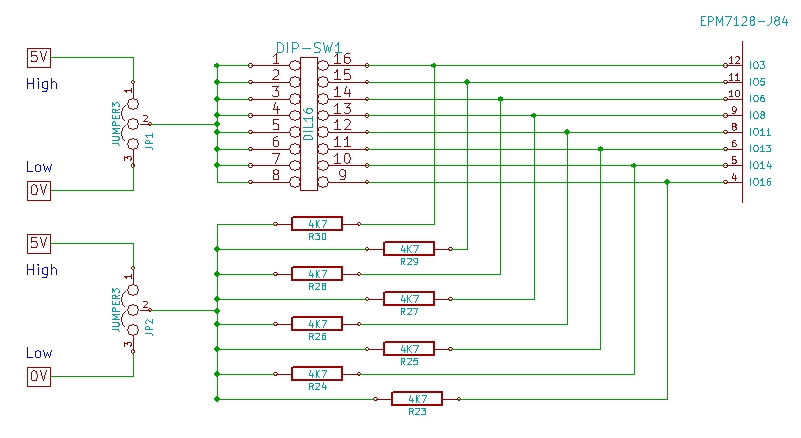
Logic Inputs : 2 x 8 bit DIP switch
packs for logic inputs (16, configurable as normally high or low,
inputs)
-
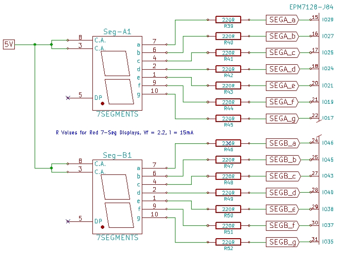
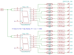
Logic Outputs : 2 x 7 Segment displays
(DP not used),
3 sets of 8 LEDs (38 total outputs)
-
Unallocated I/O : 6 Channels (wired to a
SIP header socket and available as required)
-
External power, 5VDC
-
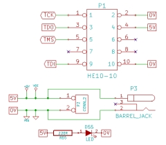
JTAG programming port
-
16MHz oscillator wired to clock input (as will be used in MTXPlus), not
required for combinatorial logic
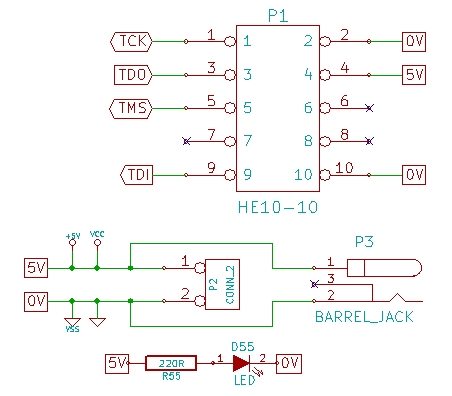
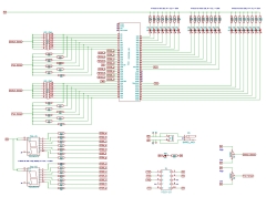
| The basic design was done using KiCad, this
is the schematic drawn before the board was
built.
While building the board, I made a small
modification - each set of DIP switches and
pull-up/down resistor sets can be individually
set high or low as required using separate
jumper blocks. |
 |
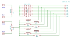
| There are two, 8-bit switch packs for the
simulation of logic inputs. Jumpers allow each
switch pack can be configured to be high or low
when the switch is closed. The CPLD input is
connected via pull/up down resistors to 5v or
0v, this is also selectable by jumper and should
be set to the opposite position from the switch
input selection. |
 |
|
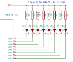
There
are three sets of 8 LEDs for the display of
logic outputs. The LEDs are in three colours,
red, yellow and green, each set has current
limiting resistors with appropriate values for
the LED forward voltage and acceptable
brightness (see below).
|
Colour |
Vf (i=20mA) |
Rc |
Ra |
|
Red |
2.1 |
145 |
220 |
|
Yellow |
2.1 |
145 |
220 |
|
Green |
2.4 |
80 |
130 |
(Vf = Diode forward voltage,
Rc = calculated, Ra =
actual)
|
 |
| There are two, 7-segment LED displays (the
decimal point is not connected), these will
allow 2 Hex digits to be displayed on the board
(with suitable VHDL programming inside the CPLD).
The 7-segment displays use red LEDs and have the
same forward voltage as the single LEDs and also
use 220 ohm current limiting resistors. |
 |
| The CPLD will be programmed on the board,
i.e., using "in system programming" through a
JTAG interface. Power will be supplied from a
standard 2.5mm DC power adapter with an LED to
indicate power is present. (The Altera
Operating
Requirements datasheet advises that 0.2uF
decoupling capacitors should be connected across
each VCC/GND pair, these have not been included
at this point.)
|
 |
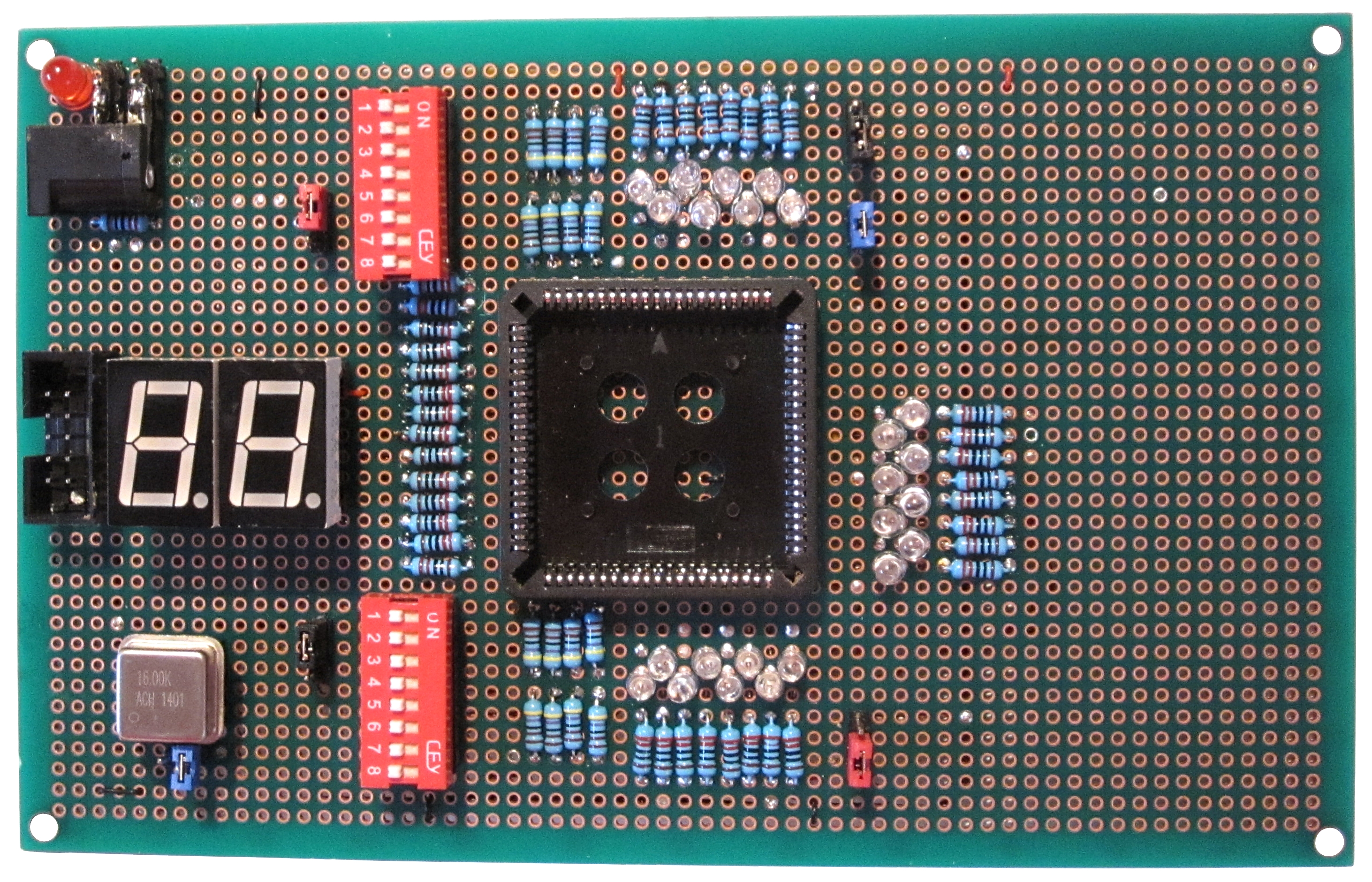
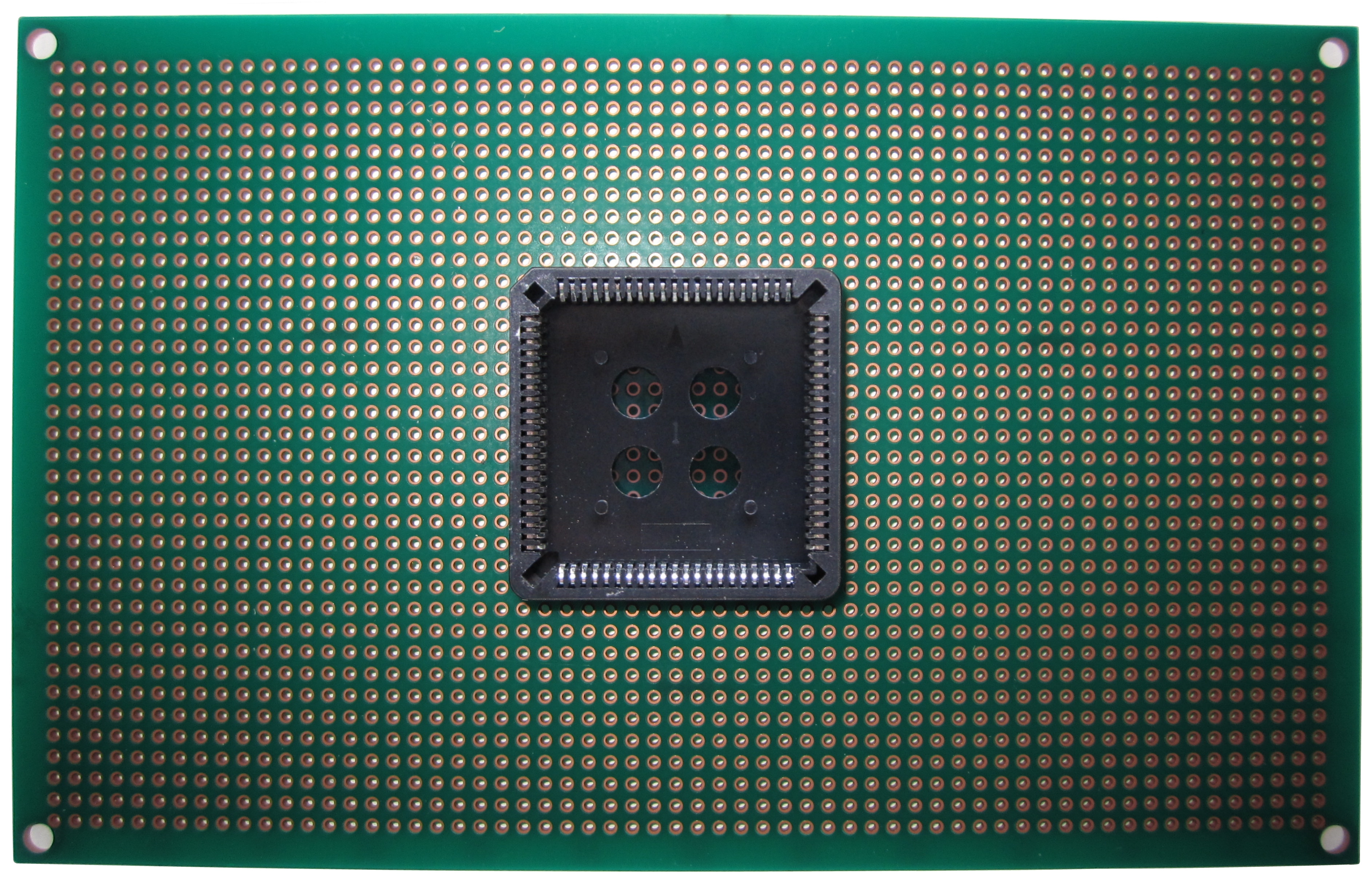
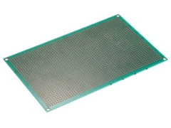
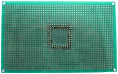
| The development board is based on this type
of prototyping board -
having just plated through holes, rather than
strip-board. The board used is the same size
as the MTXPlus PCBs will be, Eurocard size,
160mm x 100mm. |
 |
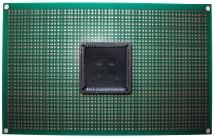
| The form factor of the CPLD that I am using
is for mounting in a PLCC-84, you can see that
the socket takes up a large area of the board -
but significantly less space than would be
required for discrete logic ships performing the
same functions. Placing the CPLD in the centre
of the board allows the most flexibility for
wiring the connections on the base of the
socket. |
 |
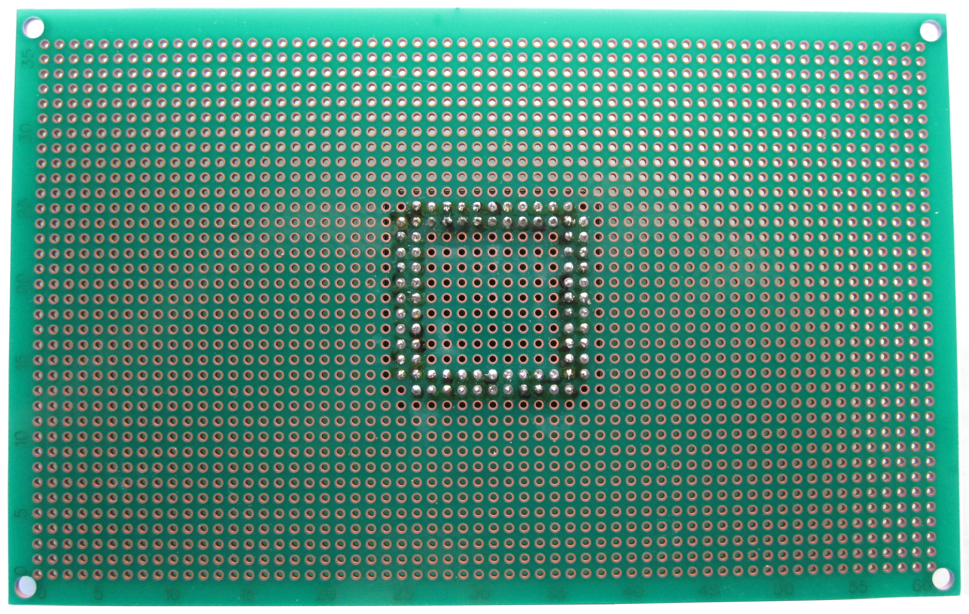
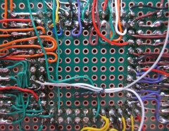
| Exposing my rather dubious soldering
"skills", the PLCC socket mounted on the
prototype board.
Adjacent pins on a typical DIP IC have a
pitch of 0.1", with pins on the opposite side
separated by 0.3". Adjacent pins on a PLCC
socket are also 0.1", but a second row is also
separated by 0.1". These tightly spaced connections are going to
present a bit of a challenge, but should be
manageable. |
 |
| Some time later . . . . . . . . . (OK then,
much, much later)
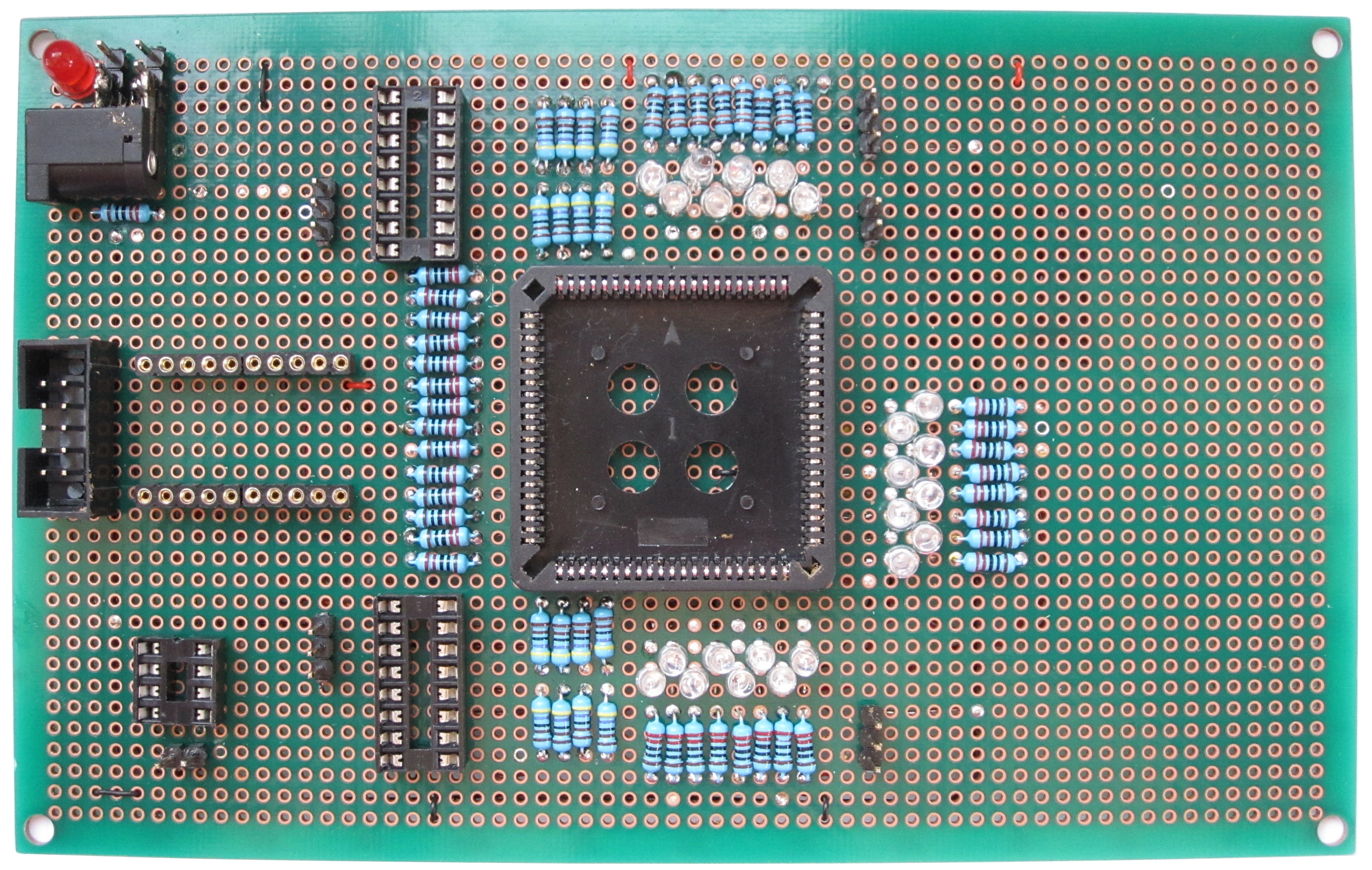
All non-socketed components mounted, i.e.,
resistors, LEDs, option jumper headers, power and JTAG connectors and the sockets themselves |
 |
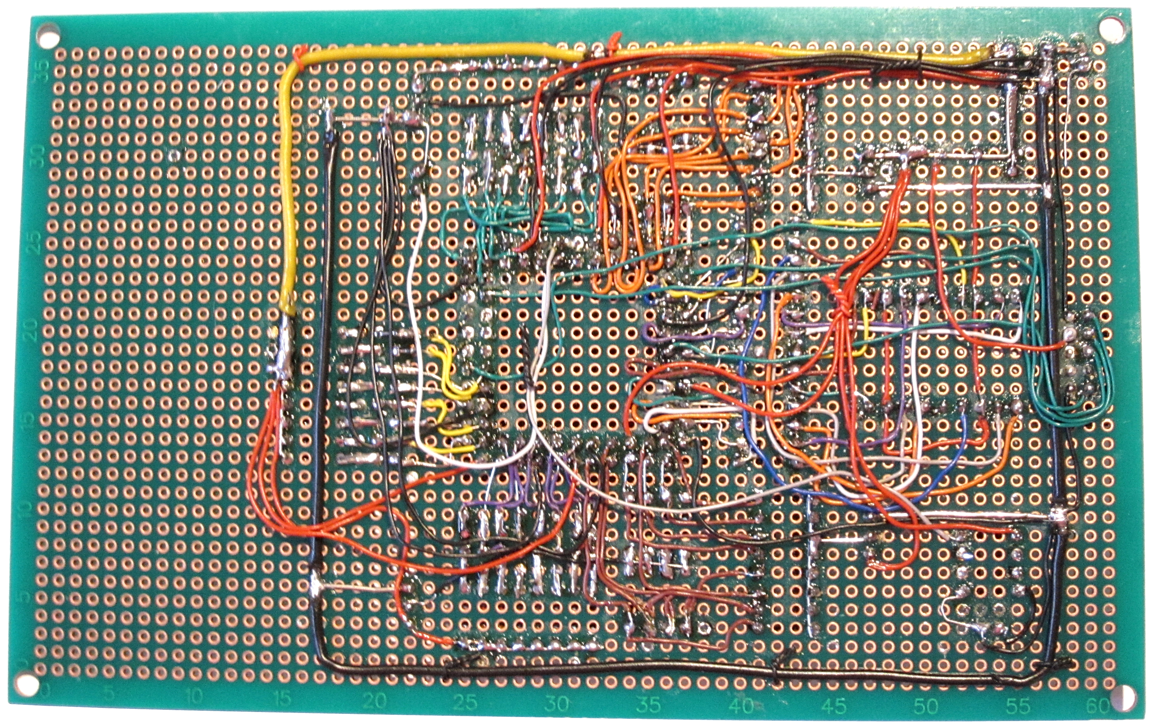
| Solder side of the board, showing my
hopefully functional, but not too pretty,
attempt at wiring it all up. Whilst wiring the
board, I found it easier to reroute a few of the
inputs to different switch positions. I have not
modified the schematic as it has no material
impact on the design - Quartus II makes pin
assignment & reassignment very easy. |
 |
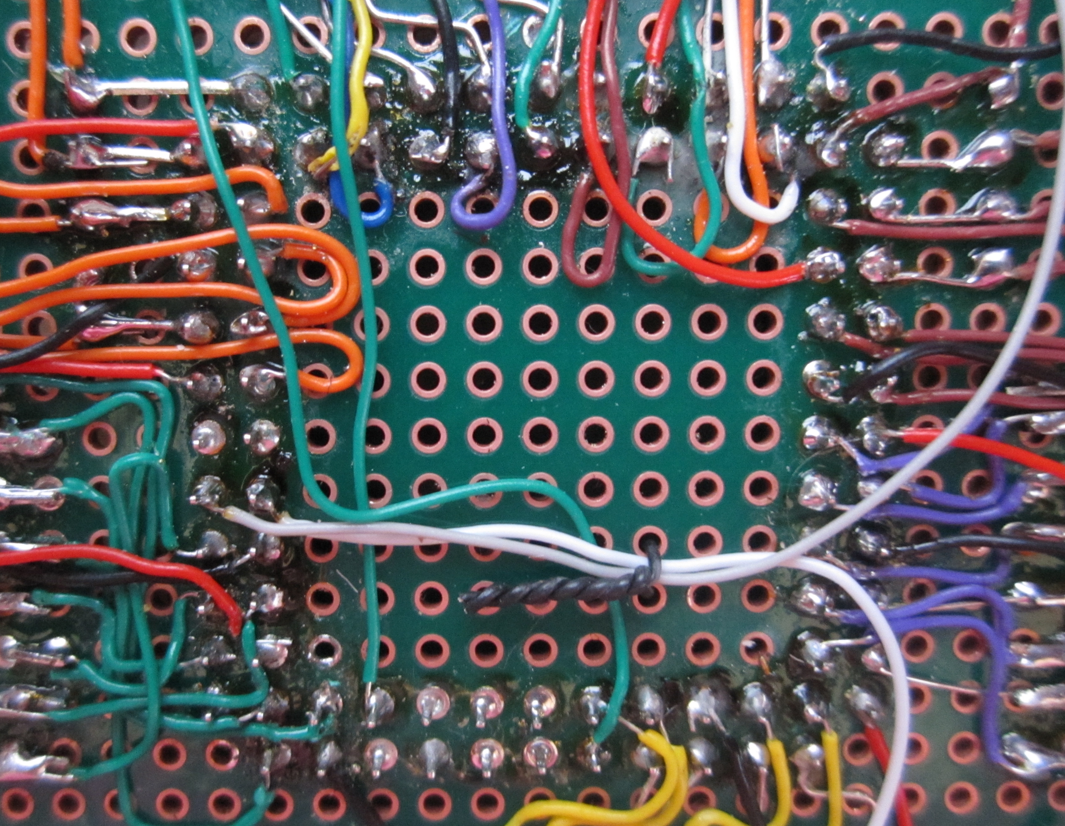
| Testing The terminations on the PLCC
socket are tightly packed and many are obscured
as later connections are made. To reduce the
potential need for rework, I did as much testing
during assembly as possible, checking for
continuity, short circuits and correct routing
from the PLCC socket contacts.
At appropriate
stages, I was able to check the I/O - the
switches, LEDs and 7-segment displays. |
 |
| Close up of the 84 connection points under the CPLD socket. Production of the development
board has been good practice for building the
MTXPlus CPU board. When I build the CPU board,
rather than connecting the external components
to the PLCC socket in turn, I think that making
all terminations at the PLCC end first will
result in a neater build, even though keeping
track of the wires may be a bit of work! |
 |
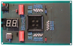
| Everything but the CPLD installed, "all" that
remains is software testing. |
 |
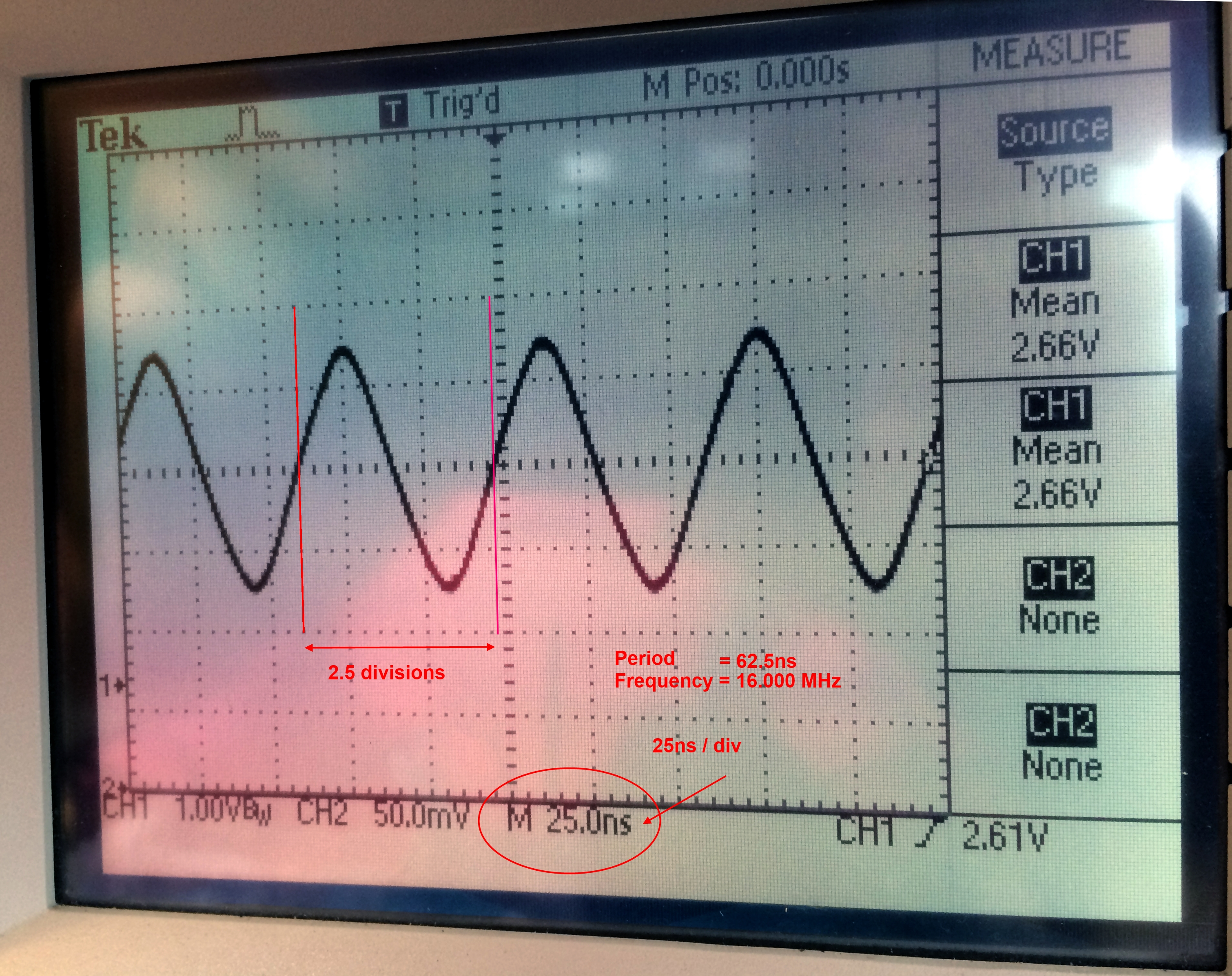
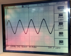
| Although not shown in the original
schematic, the silver can at the bottom left of
the i-phone photo is a 16MHz oscillator - kindly
donated by Martin. Somewhat optimistically, I
hoped that the oscillator output would be a
square wave, however, as you can see from the
'scope trace, it is sinusoidal.
I will either need to condition it on the
board or try doing it in the CPLD. |
 |
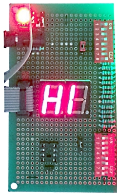
| Success - more or less . . .
Before I built the board, I did a couple of
tests with the LEDs to choose resistor values to give
what I thought to be reasonable levels of
brightness while limiting the current
appropriately.
As it
turns out, the values that I chose results in
the LEDs being a bit too bright - this makes
photographing them a bit of a problem, at
least on my iPhone. On the other hand, should I
want to start running a disco - I already have
the lighting rig!
However, while it's not quite the ubiquitous
"Hello World", at least you get the idea. The
switch packs, LEDs and 7-segment displays all do
what they are supposed to do - which, I have to
confess, was something of a surprise - no errors
with the assembly or programming at the first
attempt!
More to the point, I have been able to test
an early version of the CPU board I/O port decode
logic that I loaded as part of the first test
program - again, this works as expected. |
 |
| Design Development - I very
quickly discovered that it would be an advantage
to be able to configure the unallocated I/O on
an "as needed" basis. I have now wired the
unallocated I/O pins to a SIP socket where they
are available for use as required. I don't
imagine that anyone will want to build a board
the same as mine, but for completeness, I need
to do an "as-built" schematic of the board, I'll
get to that shortly. |
<-----
To do |
|
Comparison With Altera
UP1/2 Development Boards |
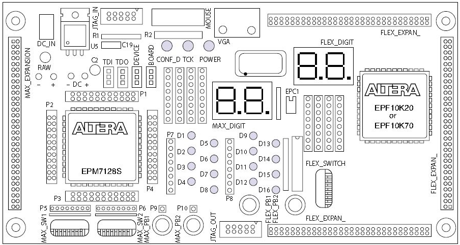
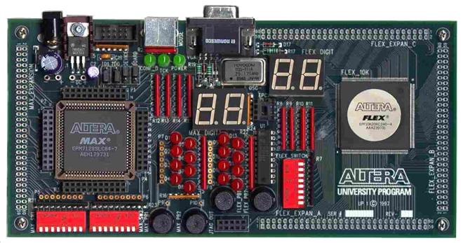
| Layout of the Altera UP1 and UP2 boards, you
can see that the left hand side of the board has
very similar features to mine, including DIP
switches, LEDs and 2 x 7-segment displays. |
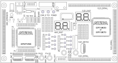 |
| A photo of a UP2 board, obviously looking
far better than mine, but these boards are
obsolete, not readily available and would in any
event, be far more expensive than my version. |
 |
MAX7128S Timing <
Previous
Page Goto
Next
Page >
MAX7128S Programming
|