|
"MTX Plus+" -
Diagnostics Card
Early computers such as the DEC PDP 1 (pictured), had
impressive front panels with lots of switches and flashing
lights to control and display the operational status of the
machine. Sadly, modern computers don't feature such interesting
operator interfaces, some might say that they are not required
and would serve no useful purpose in a modern day, or even
1980's vintage, computer, but in my opinion, you can never have
too many flashing lights :-)
I am big fan of flashing lights - useful or not, and
needed to find a good excuse to put lots of lights on MTXPlus.
In the early stages of development, there is likely (hopefully)
to be an operational CPU board before a video board is available
and I want to be able to determine whether the CPU appears
to be running "stand-alone" with no operator interfaces
connected.
Bus Diagnostic Card
So, killing two birds with one stone, there is now an
MTXPlus Bus Diagnostic Card, although with "slightly" less
functionality than a PDP-1, but then, it is a fraction of the
size and cost!
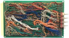
As you will see, I have gone overboard (again), the board is
much more complicated than it needed to be to just monitor the
status of the MTXPlus bus signals. Martin's board has all of the
required functionality, but is much less complicated - see the
photos at the bottom of the page.
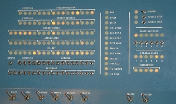
The board uses a number of 7-segment displays and single
LEDs to display the Z80 Address and Data bus status', as well as
the status of the Z80 control bus and miscellaneous MTXPlus
signals. The card also has a reset toggle switch to allow a
hardware reset to be applied to the CPU and other chips with a
RESET input.
In a "late design change", I included a single step
instruction circuit that I had seen on the
Z80 Computer
Project blog. The
Single Step Instruction Circuit page on the blog describes
the purpose of this function and how the circuit works In brief
. . . .
"While debugging you may find you would like to step
through each instruction executed to assure that the
function of your system is correct. Instead of cycling the
clock over and over to get through each instruction with a
single-step clock circuit, a new circuit can be built to
receive a de-bounced button press, and then execute one
instruction at the speed the Z80 is set to run at. This
requires a single-step instruction circuit. To build such a
circuit we will be exploiting two control signals on the
Z80, WAIT
(Pin 24) and
M1 (Pin 27)."
(For a complete explanation, refer to the description on
the
Z80 Computer Project webpage, but I have also captured a
copy on the
notes page.)
|
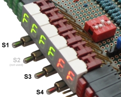
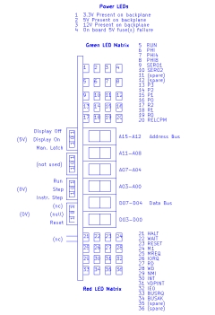
Switches & Jumpers |
|
Switch |
Position |
Description |
|
S1 |
Latch |
Display & Bus Status LEDs Off |
|
Null |
Display & Bus Status LEDs On |
|
Mmnt |
7-Segment manual latch (see
below) |
|
S2 |
(spare) |
Not used |
|
S3 |
Latch |
CPU
in normal (RUN) mode |
|
Null |
CPU
in Instruction Step mode |
|
Mmnt |
Step
Single Instruction |
|
S4 |
Latch |
Not used |
|
Null |
CPU
Reset "normal" position |
|
Mmnt |
CPU
Reset (drives
RESET
low) |
|
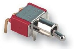
Toggle Switches
 |
|
You may have noticed a number of
jumpers in the photos, these were put in to give
me some flexibility should the planned design
have problems, these jumpers turned out not to
be needed, but for completeness, I will explain
their purpose. |
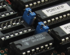
Option Jumpers |
|
I didn't have a SPST toggle
switch to hand when I built the board, so I made
a change to the Instruction Single Step (ISS)
circuit by adding an inverter and doing some minor
wiring changes.
In case this modification did
not work, to give me the flexibility to revert
to the original ISS design without needing to do
potentially awkward wiring changes after the
board was built, these jumpers were included so
that the original design could be implemented by
just adding a new switch.
Now that the SSI circuit has
been tested, they are just left as shown. |
 |
|
During the build, I got a little
concerned about the power consumption of the
display elements and the current rating of the
Kynar wire that I was using. The 3 x 3-pin
jumpers were installed to make redistribution of
some of the 5V load easier without substantial
rewiring. Again, this turned out not to be a
problem, so the jumpers are just left as shown.
The yellow jumper allows the
PDN747 blanking input to be controlled by the
display On/Off button, or tied low to have the
7-segment display always on. Again, this is not
actually required and can be in either position. |
 |
|
Power Supply |
| Function |
Indicator |
Description |
|
| Fuse Failure |
LED |
Fuse failure on one or more
board +5V lines |
 |
| +5V |
LED |
+5V Supply present on backplane |
 |
| +12V |
LED |
+12V Supply present on backplane |
 |
| +3.3V |
LED |
+3.3V Supply present on
backplane |
 |
|
LED Status Indications |
|
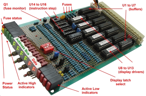
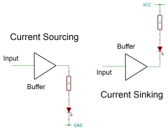
On the diagnostic board, the TTL
signals on the backplane are buffered by
74LS24x buffer/line driver chips before being
used to drive the LEDs and displays.
Due to the way that TTL devices
are constructed, a TTL output can typically
"sink" more current than it can "source", for
example, the National Semiconductor 74LS240/241
datasheet shows that the maximum source current
per output is 15mA, whilst the maximum sink
current in 24mA. Therefore, when driving loads
such as LEDs, the preferred option is to use
current sinking. |
|
In simple terms, in current
sourcing, the current supplied to the load comes
from the chip. In current sinking, the current
supplied to the load comes from
VCC and is merely switched by the
logic chip.
There is a slight issue with
this though, intuitively, we think of something
as being "ON" when at Logic "1". For a
non-inverting buffer, such as the 74LS244 in
current sinking mode, turning on the LED
requires that the input to the buffer is a Logic
"0" to allow the current to flow. Using a
73LS240 (inverting) buffer means that a Logic
"1" on the buffer input becomes a Logic "0" on
the output, allowing current to flow and the LED
to be illuminated. |
 |
|
Z80 Control Bus Signals |
| The signals on the
Z80 control bus are active low,
i.e., are normally "1" and are "0"
when in the active state. The
function and operation of these
signals is described in the Zilog
Z80 Databook, you can find a copy in
my Technical Library pages
here. (The Z80
RFSH
signal is used to initiate the
refresh of Dynamic RAM and will not
be used in MTXPlus which uses Static
RAM.)
The status of these active low
signals are indicated by
RED LEDs, when the signal
is active, the corresponding LED
will be ON, when the signal is
inactive, the LED will be OFF.
In this case, the LEDs are
driven by 74LS244 non-inverting
buffers as the LEDs are intended to
be OFF when the signals are
inactive, i.e., at Logic "1". |
|
Z80 Control Signals |
|
BUSRQ |
Bus
Request |
 |
|
BUSAK |
Bus
Acknowledge |
 |
|
NMI |
Non-maskable
interrupt |
|
|
INT |
Interrupt Request |
|
|
WAIT |
Wait |
|
|
HALT |
Halt |
|
|
RESET |
Reset |
|
|
MREQ |
Memory
Request |
|
|
M1 |
M1 Cycle |
|
|
IORQ |
I/O
Request |
|
|
RD |
Read
Data |
|
|
WR |
Write
Data |
|
|
RFSH |
Memory Refresh (not
used) |
|
| |
To the
Z80 CPU |
|
| |
From the
Z80 CPU |
|
|
|
|
MTX / MTXPlus Specific Bus Signals |
|
VDPINT is the
interrupt signal from the VDP to the
CPU
IEO
is used to prioritise daisy chained
devices that can interrupt the CPU
through the
INT
line. In the MTX computer, the
highest priority daisy-chained
interrupt is from the CTC, the CTC
Interrupt Enable In (IEI)
line is connected to +5V ensuring
that it has the highest priority.
The CTC Interrupt Enable Out
(IEO) line is connected to the DART
IEI line.
The status of these active low
signals is indicated by
RED LEDs in the same way
as the Z80 Control Signals.
The remaining signals are
specific to the MTX/MTXPlus, these
signals are active in the high
(logic "1") state and their status
is indicated by
GREEN
LEDs. |
|
Custom Backplane Signals |
|
VDPINT |
VDP
Interrupt |
|
IEO |
Interrupt
Chain |
|
PHI |
System
Clock |
|
PHI4 |
4
MHz Clock |
|
PHI8 |
8
MHz Clock |
|
SER01 |
Serial
Channel A Clock |
|
SER02 |
Serial
Channel B Clock |
|
P0 |
Page
Port (RAM page select) |
|
P1 |
Page
Port (RAM page select) |
|
P2 |
Page
Port (RAM page select) |
|
P3 |
Page
Port (RAM page select) |
|
R0 |
Page
Port (ROM page select) |
|
R1 |
Page
Port (ROM page select) |
|
R2 |
Page
Port (ROM page select) |
|
RELCPMH |
Page
Port (ROM/RAM mode
select) |
|
|
|
Z80 Address and Data Buses |
|
The simplest method of displaying the status of
the Z80 Address and Data bus signals would be to
have a single LED per signal, in the same way as
for the control signals. Although not really
necessary, I decided that I wanted to decode the
address line and data line signals and present
the actual address and data values on 7-segment
displays.
A single 7-segment display can display the data
for up to 4 binary inputs using 16 hex
characters, 0,1 2, 3, 4, 5, 6, 7, 8, 9, A, b, C,
d, E, F.
The binary inputs must be decoded to determine
which of the 7 segments should be illuminated to
display the character corresponding to the
inputs. |

Image from:
Frederick Blais blog |
|
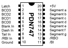
This was somewhat problematic,
whilst Binary Coded Decimal (BCD) to 7-segment
display drivers are common, Hex to 7-segment are
not. Typically, a ROM or microprocessor based
solution is used to translate the binary inputs
into the appropriate code to be passed to the
7-segment display.
After much searching, I managed
to source this chip, a PDN747, from the US. The
cost of the chips, plus shipping & VAT, as well
as the cost of the 7-segment displays makes it
more expensive and requires a larger footprint
on the board, but I think it's a nice feature. |
 |
|
There was a
minor problem with the PDN747 though, the device
needs a latch signal to clock the BCD inputs to
update the displays. The dip switch pack
provides a number of latch selection options:
| 1 |
Latch on the rising
edge of the clock signal (PHI) |
| 2 |
Latch on the rising
edge of
M1 |
| 3 |
Manual latch, using
toggle switch S1 momentary position |
| 4 |
Latch signal from
the backplane (DIAG) |
|
 |
|
Power Considerations |
|
The board features quite a
large number of discrete LEDs and 7-segment
displays, potentially resulting in a relatively
high power demand, for example, 35 single LEDs
and 48, 7-segment display elements (6 x 8,
including DPs) , each drawing 20mA would give a
power requirement of some 1.7A, not including the load
from the ICs and pull up/down resistors.
The
backplane
design includes one pair of pins for 5v
power distribution, the DIN connector pins are
rated at 2A, allowing up to 4A of 5v power to be
supplied to each board - adequate for the worst
case load. However, the board interconnections
are made using 30 AWG
Kynar wire, the type that I am using was
advertised as being rated for 0.5A but I believe
that this may be an error, a more typical rating
for Kynar wire is
0.4A, so consideration needs to be
given to how power is distributed around the
board. It would have been ideal to have larger
capacity conductors on the board for the 5v and
ground lines that could form a power bus to
which individual terminations could be made -
kind of like a
ring main, but I didn't think that the size
of the board and component density would make
that very easy.
Instead, I chose to use a number
of radial 5v and ground lines, tied back to
single points at the connector pins and
distribute the power in sections. Given that it
would be possible to overload the conductors, I
installed fuses in each of the power lines.
Ideally, the fuses should have been sized to be
less than the conductor current rating, but I
chose to make them the same, i.e., 400mA.
Although not representative of
the power consumption, the radial power lines
are installed on a board layout basis
| Column |
Components |
Fuse No. |
Fuse Size |
| A |
LS240/LS244 Buffers |
1 |
400 mA |
| B |
PDN747 Display
drivers |
2 |
400 mA |
| C + E |
Misc logic,
7-segment displays |
3 |
400 mA |
| E |
Discrete LEDs |
4 |
400 mA |
The 7-segment displays produce
good brightness levels using a current of ~10mA,
with all segments and the DPs illuminated, this
would require about 480mA, but there will be
some degree of diversity depending on the values
being displayed at a given time. When displaying
values of 0 to Fh the average number
of segments illuminated is ~5, so, assuming that
the numbers being displayed are random, the
current would be ~300mA.
Due to space constraints, the
board uses stacked LEDs that allow 4 LEDs to be
installed in a very small space, there was a
trade-off between the space saving and the
current consumption of the LEDs. The current
required to produce an acceptable level of
brightness is higher than the current required
with a "normal" LED, I found that 16mA produced
an acceptable brightness for each of the colours
being used. The power requirement of the LED
modules will be 35 x 16mA, i.e., 560mA, but
again, some degree of diversity will apply; the
LEDs will only be on when the associated signal
is active, looking at the signals involved, an
on time of 50% would seem to be a reasonable
assumption, leading an estimated current
requirement of ~280mA. (When the bus is not
being driven, the logic inputs will float and
likely drift high. The LEDs turned on by a logic
"1" will illuminate, but as this is only 50% of
the available LEDs, this is not likely to be a
problem either.)
If the current drawn by the
indicators proves to be higher than the fuse
rating, it would be relatively easy to rewire a
couple of the 7-segment displays to take power
from one of the lightly loaded lines feeding the
ICs, but I will leave things as they are unless
it proves to be a problem. |
|
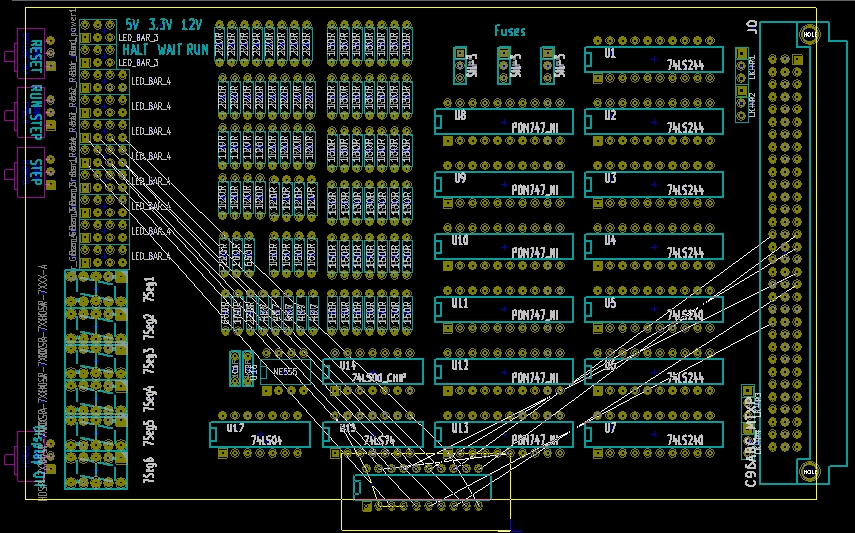
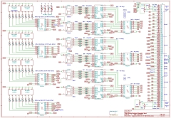
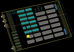
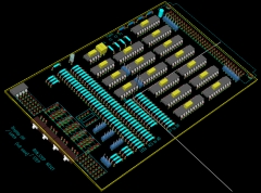
Board Design |
|
This is the "as-built" design of the
diagnostic board, as a result of the 7-segment
displays and associated logic, the board is now
much more complex than I originally envisaged.
(v1.03)
The schematic is drawn with
KiCad, but the prototype (1-off ?) board is
constructed on a eurocard sized prototyping
board. |
 |
|
At this stage, the board was not
going to be a PCB, it was constructed on
prototyping board and the "tracks" are wire
links.
Nevertheless, the KiCad layout
and routing tool (PCBnew) was very useful in
optimising the placement of the components. It
was also useful to see the required wiring paths
when moving components around to see if I could
optimise the wiring too. This is an early
version of the layout before I settled on the
final design shown below. |
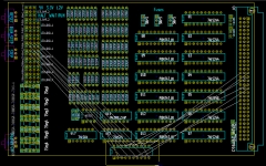 |
|
The layout for the
diagnostic board, as you can see, the components
all fit on the Eurocard sized board (160mm x
100mm), but there is not a lot of free space and
wiring it up was quite a challenge!
The other challenge was how to make sure that
all of the indicators and switches were
accessible from the end of the board,
particularly if the computer ever makes it into
an enclosure. |
 |
|
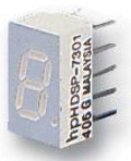
7-segment displays have a much
larger footprint than equivalent single LEDs,
but I was able to minimise that by using 0.3"
displays and making them visible from the end of
the board by using right angled sockets.
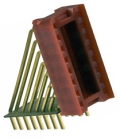
The sockets are
Series 800 Vertisockets, manufactured by
Aeries
Electronics, these are quite expensive new
(~£10). I was able to source some "pulls" from
Israel for ~£1.50 - fitted with red displays. |
  |
|
There are also around 36 single
LEDs needed for the Z80 control bus signals,
MTXPlus backplane signals and power indicators.
To optimise the available space on the front of
the board, I used 2 x 3mm quad-level LEDs |
  |
|
There are also a number of
switches that need to be accessible from the
front of the board.
They are mounted directly below
the display sockets. This was possible since
positioning the sockets to align the displays
with the quad level LEDs left three unused
columns of holes below the socket. |
 |
|
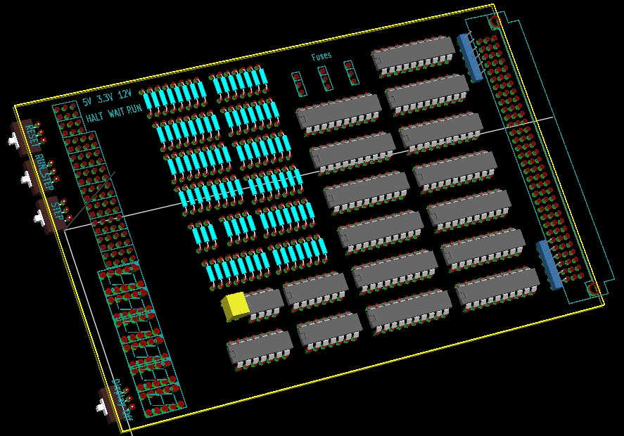
A PCBnew 3D view of the
components placed in their locations during the
design phase.
Although I don't have 3D models
for the 7-segment display vertical sockets or
the stacked LED modules that I used, the model
did give a good indication of how the finished
board would look. |
 |
|
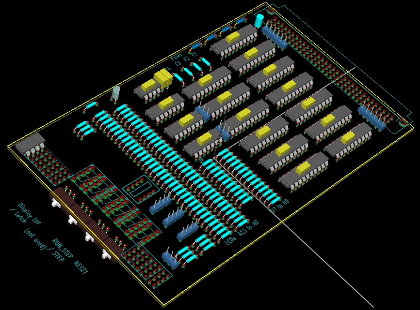
This image is of the "as-built"
board which includes the various minor
modifications made during the build but does
show that the finished article looks very much
like it was supposed to.
This one also includes the
decoupling capacitors installed inside the
sockets of the ICs - the model is a bit
misleading in that respect - it looks like they
are sat on top of the ICs - obviously, this
isn't the case. |
 |
|
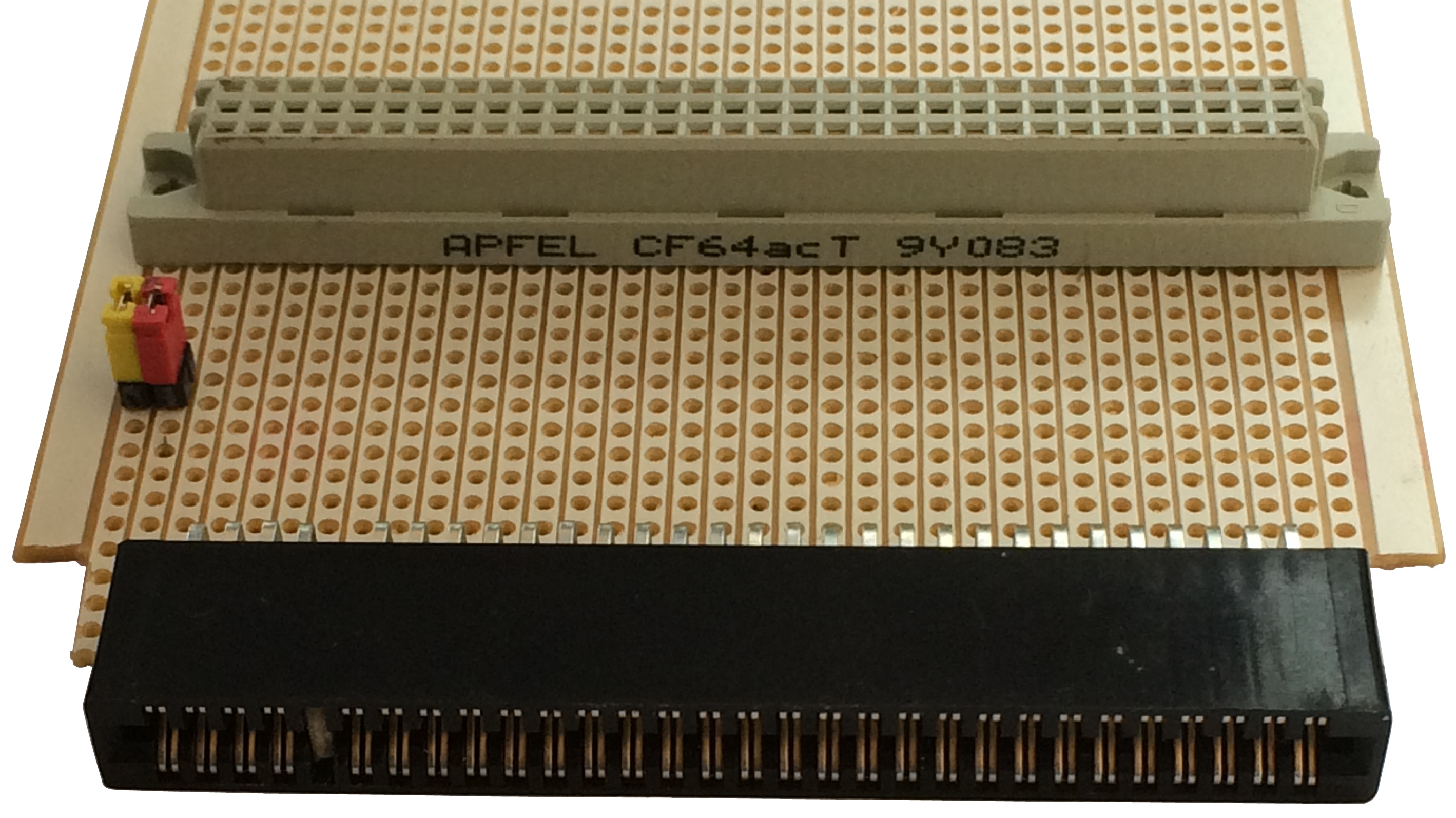
Construction |
|
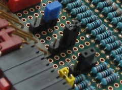
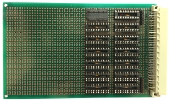
The diagnostic board starting to
take shape, the sockets closest to the DIN 41612
connector are for 74LS240/244 buffers and the
adjacent sockets are for the PDN747, 7-segment
display drivers.
You should be able to make out
the decoupling capacitors installed inside the
DIP sockets to save a little board space. The
layout layout is a little
different to the original layout drawing - I did
some optimisation as I placed the components -
the schematic drawing has been updated to
"as-built". |
 |
|
A view of the solder side, with
only the power and ground connections to the DIP
sockets and decoupling capacitors made so far. |
 |
|
Some progress - the Address
lines (A0-A15) wired up to the LS244 buffers and
onward to the 7-segment display drivers.
The incremental difference in
the photos does not do justice to the effort
required to get to this stage! I am reasonably
confident that the wiring to this point is OK -
at least, checking with a meter, it agrees with
the schematic. |
 |
|
Another update - the blue and
green bundles are the output signals from the
LS240/244 buffers that will control the red and
green LEDs in the quad level LED modules. |
 |
|
At around this point, the
hex-to-7-segment display drivers that I had
bought finally arrived from the US and I was
able to test one. Things did not go quite as
well as hoped (you can find the details on the
notes page)
and I need to make a small modification to the
wiring of the PDN747 sockets and add a little
logic to control the update of the 7-segment
displays. In the following
pictures you will also notice that the position
of the single step circuit components and the
orientation of the LED current limiting
resistors is different to the schematic - I made
a number of changes when I added the latch logic
for the PDN747s. |
|
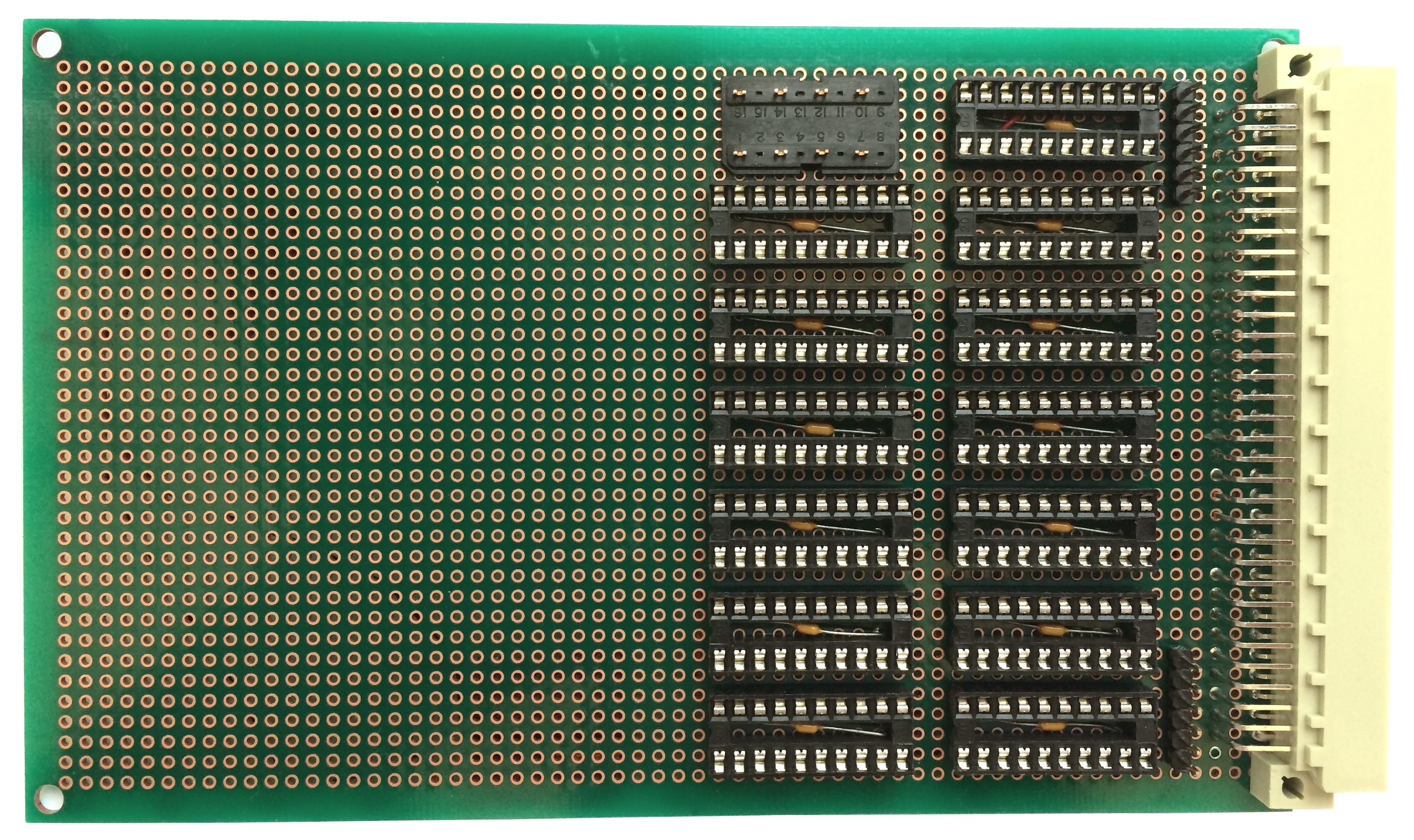
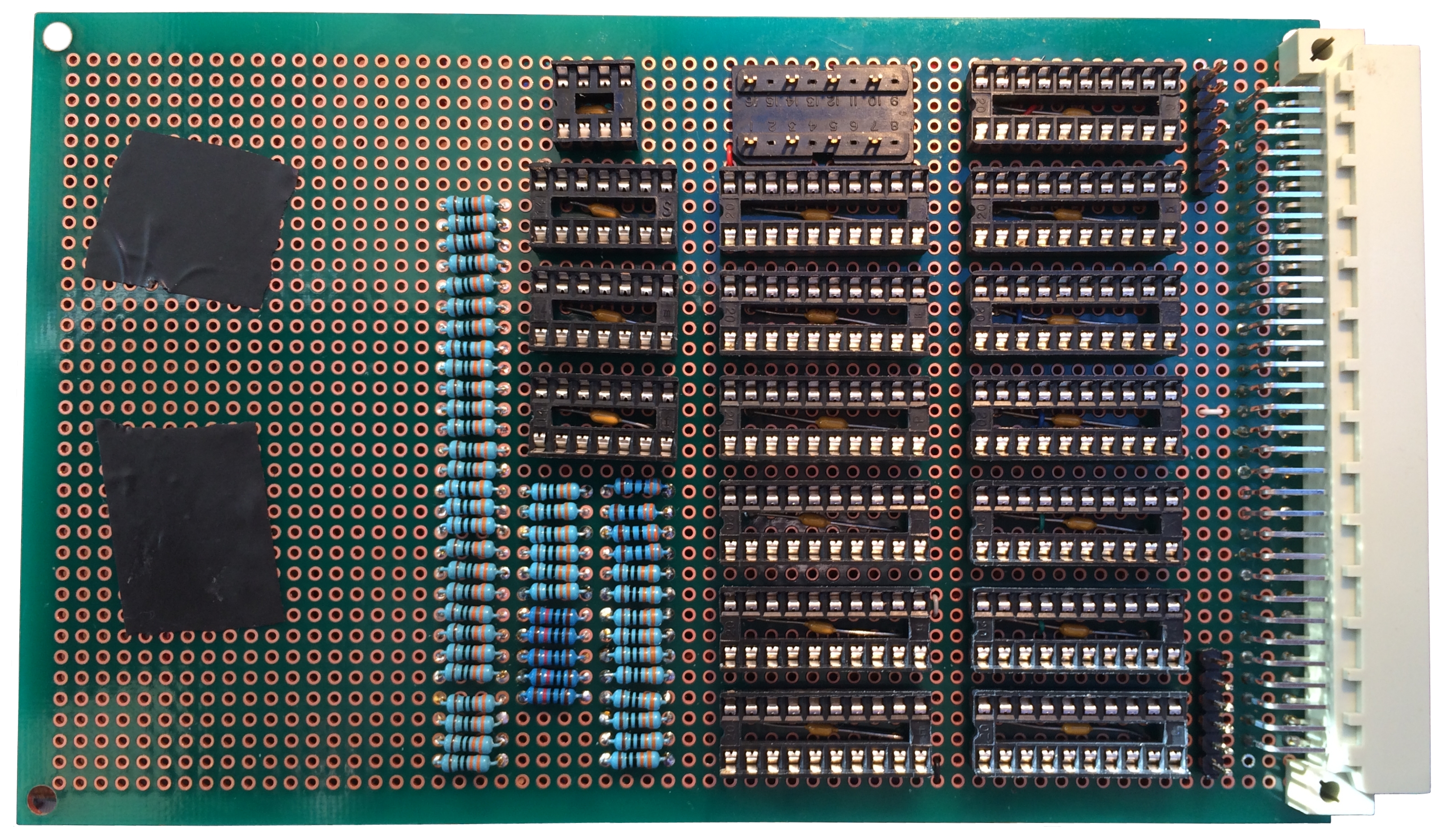
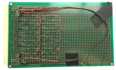
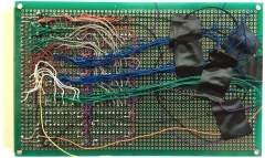
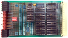
The rest of the sockets mounted;
the top 3 are for the single step instruction
circuit and the one below them is a 74LS04 for the
7-segment latch logic.
The 5 x 10K resistors are
pull-ups for the single step circuit and the 48
x 330R resistors are for the 7-segment displays
(including the decimal points). That "only"
leaves another 36 resistors, the display
elements and switches to be added! |
 |
|
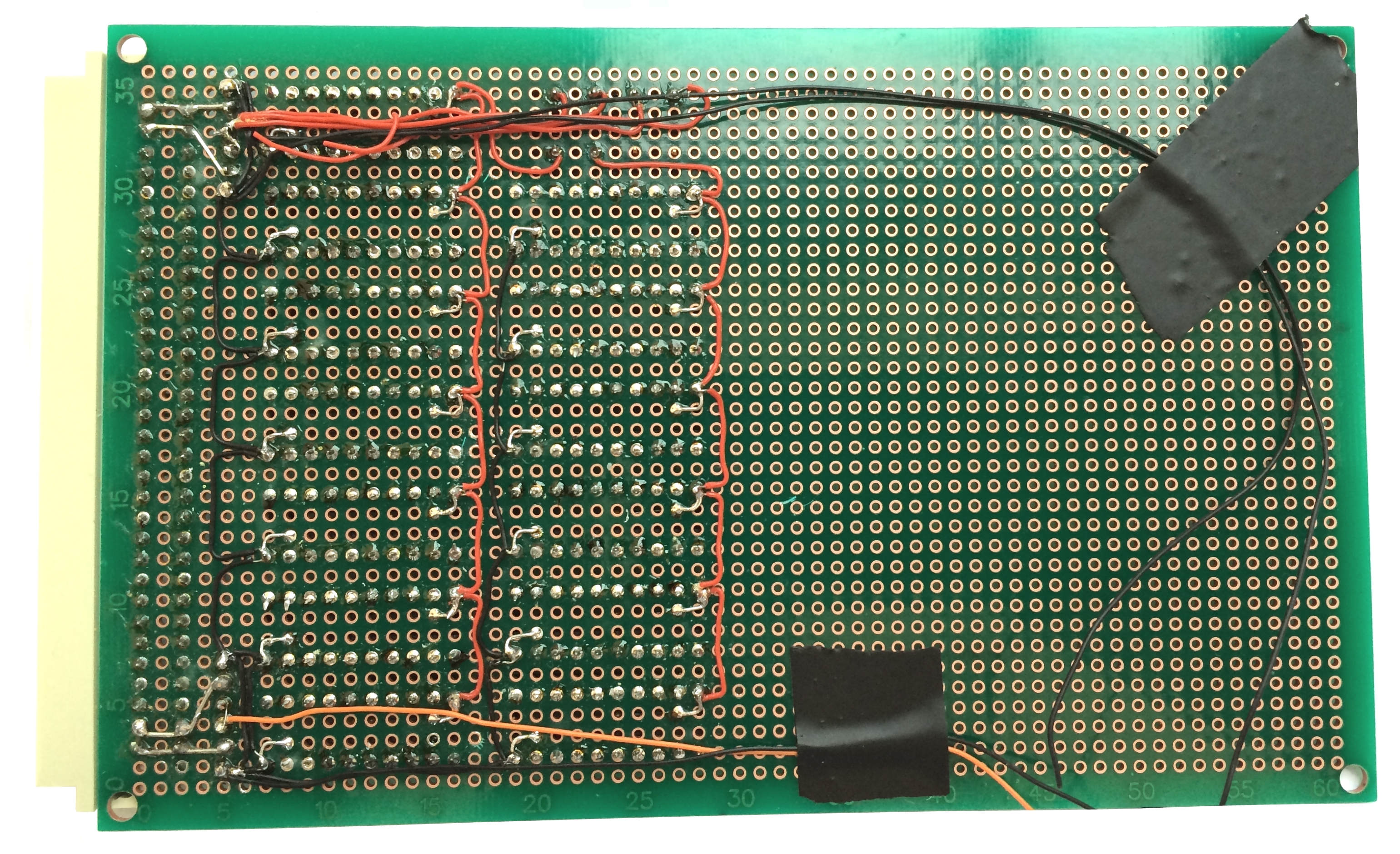
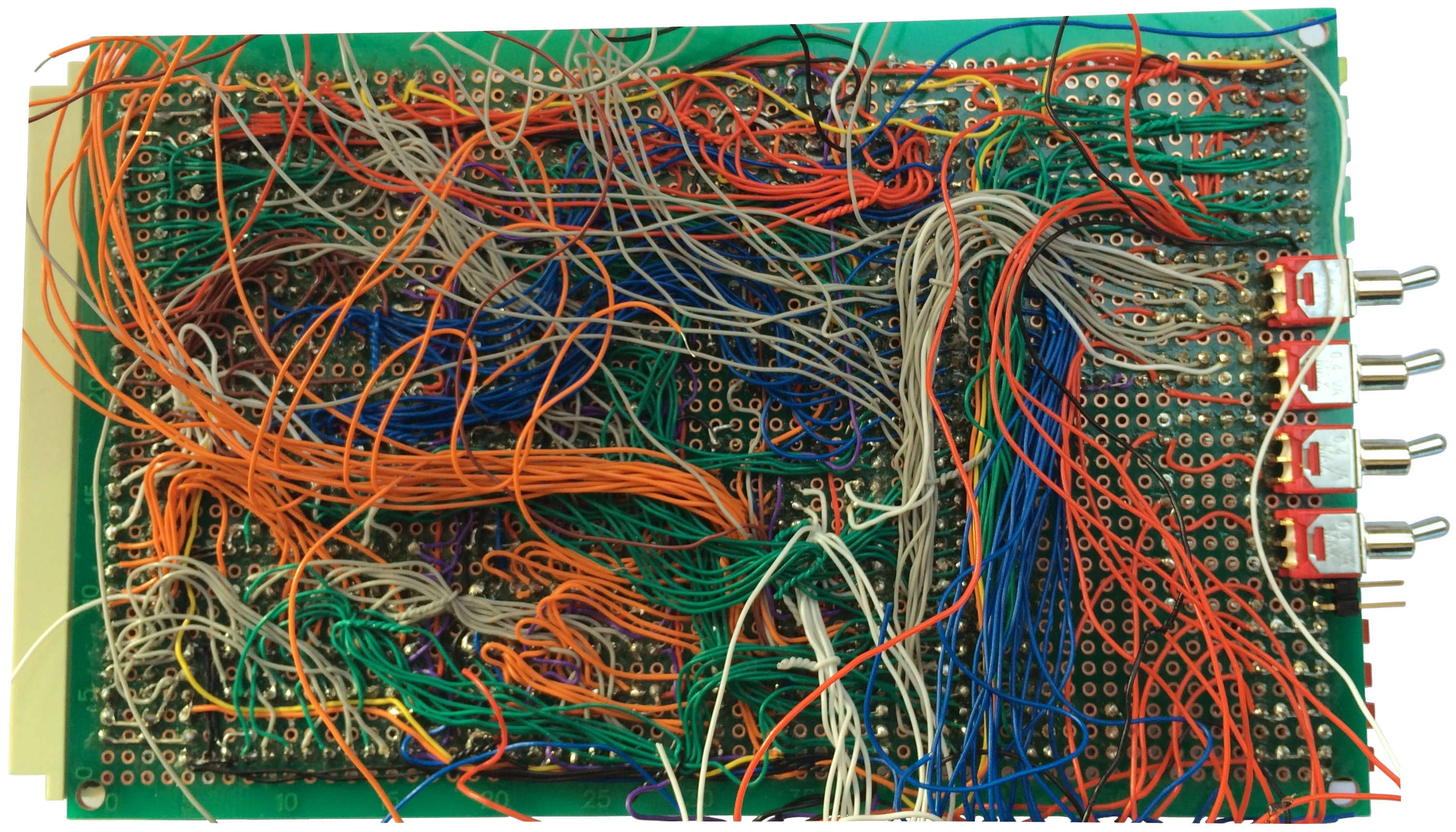
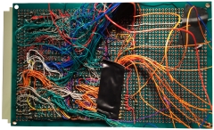
The left hand side of the board
is now almost fully wired.
There is an interesting
dichotomy when doing the wiring, making the
wires as short as possible makes the board look
neater, but would be problematic should any
rework be necessary. I tried to leave a little
slack on most of the connections, but the need
for rework should be minimised as I am testing
the connections at convenient stages. |
 |
|
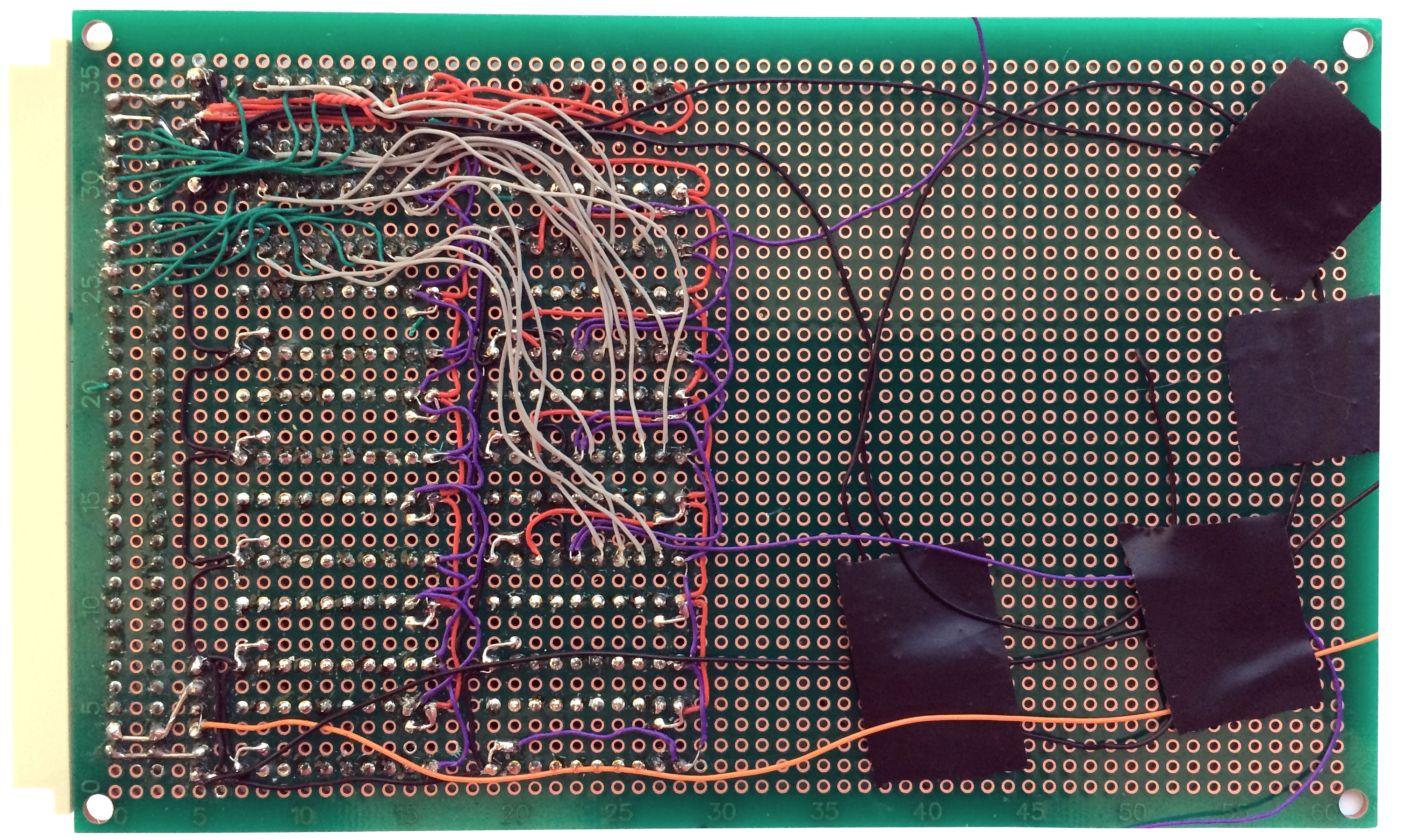
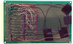
Getting there!
- The obvious difference from
the last photo are the additional column of
resistors for the 4 level LED modules, the 4 x
10K
pull-downs and diodes for the fuse monitor
circuit as well as the capacitors for the single
instruction step circuit. |
 |
|
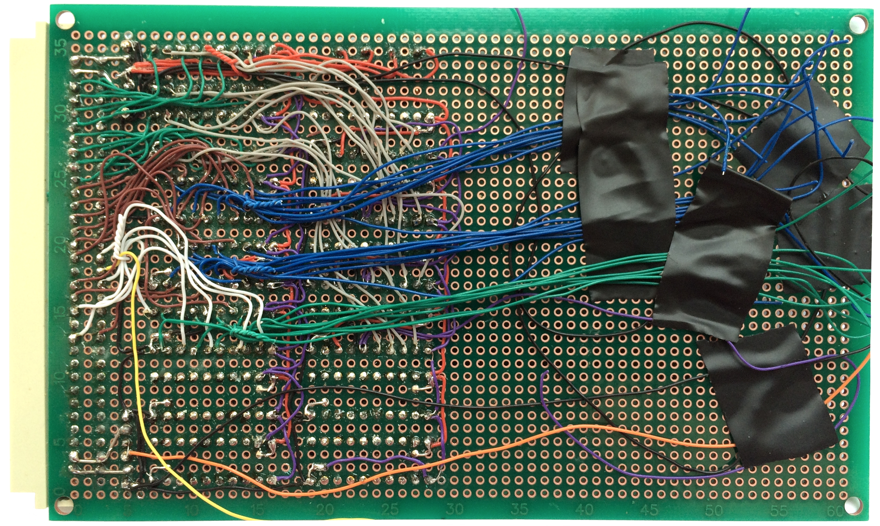
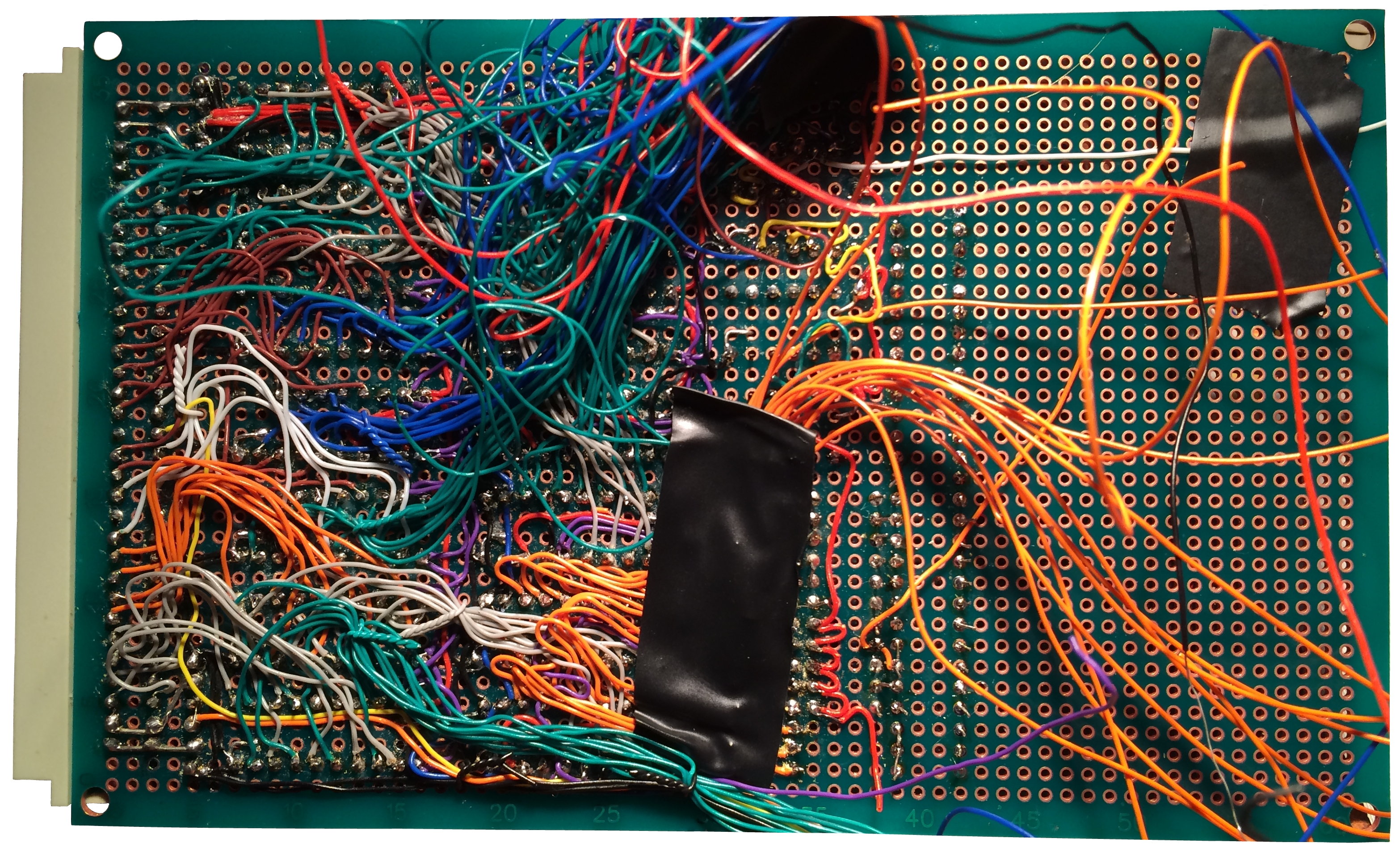
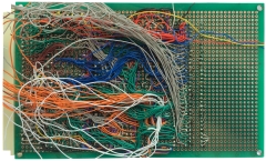
Just for completeness . . . . .
. the solder side of the board.
Still looking a bit of a rat's
nest, but there is some structure to it -
honest! All that remains is to mount the
displays and switches, then connect them up to
the unterminated wires and resistors. |
 |
|
The last of the components
mounted, just a hundred or so connections left
to solder now!
The black modules at the left
hand side are the quad level LEDs and the odd
looking right angled sockets are for the
7-segment displays. You can also see the toggle
switches mounted on the underside of the board. |
 |
|
To allow the switches to be
mounted in the holes below the display sockets,
the switch contact legs and securing posts were
trimmed so that they were flush with the top
side of the board. This will result in the loss
of some mechanical strength, but I don't think
that is significant here. |
 |
|
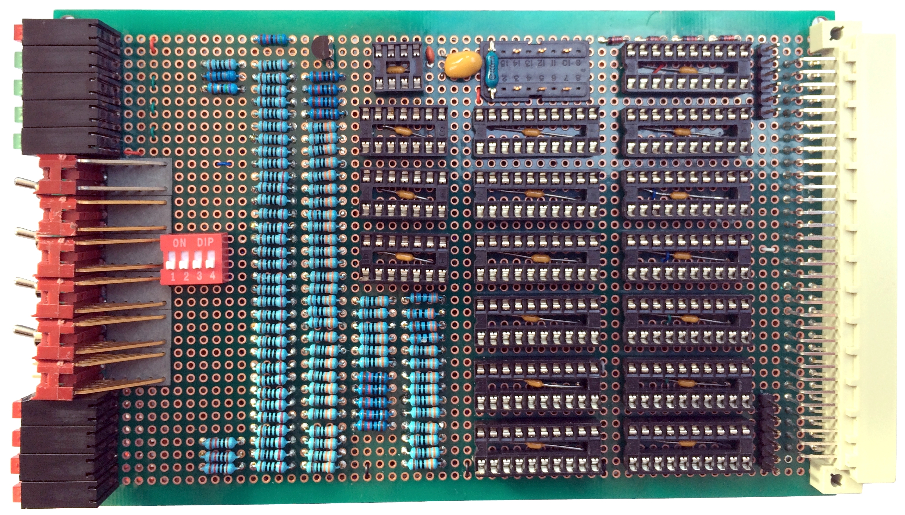
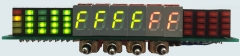
Completed - ready for testing |
|
The completed board with all
components, apart from the single instruction
step ICs, installed. The board is being powered
by a temporary supply which provides only 5VDC.
The address and data bytes are
all reading "FF" as the bus signals are floating
and currently "high", i.e., each bit is
currently interpreted as a "1".
The board has been tested and appears to work as
required (after fixing a problem that I had
created when choosing the value used for the
chip enable pin pull-down resistor - more
details on the
notes page). |
 |
|
The red LEDs are all off (the
active low signals have floated high) and the
green LEDs (apart from the two spares tied to 0v) are all
on (high). |
 |
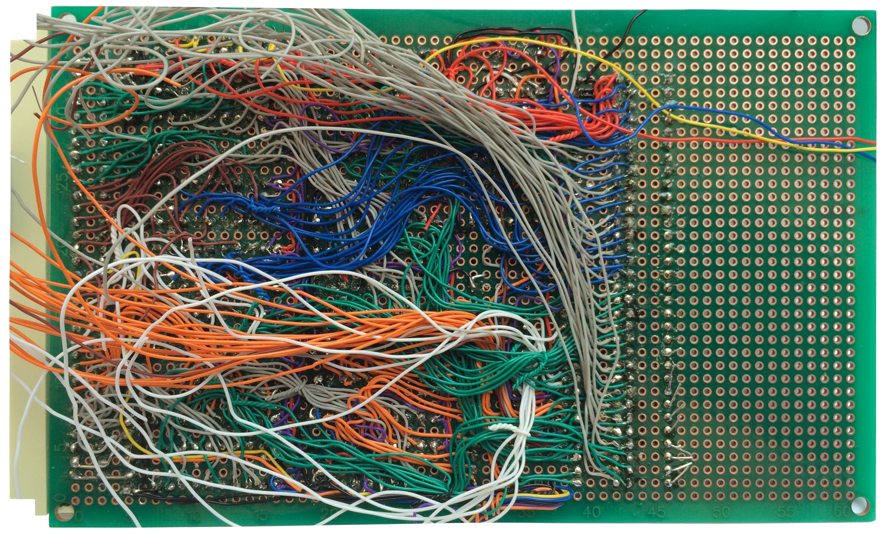
|
The "final" state of the solder
side of the board, still not looking too neat!
There are a number of spare wires that
are not fully terminated and the slack left in other
wires means that it does not look very tidy, but
it's the best that I could do. I will probably
spend a little more time tying up the wires to
make them a bit more secure though. |
 |
|
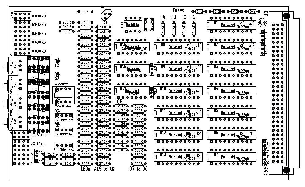
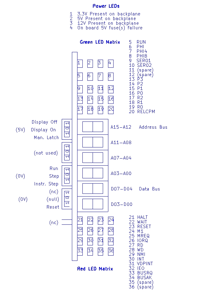
"Crib Card" for my benefit . . .
. .
Showing the position and function of the
various LEDs and switches, it's a poor quality
drawing, being done in KiCad during the
schematic design phase, but it does the job.
I'll probably do a decent drawing at some
point. |
 |
|
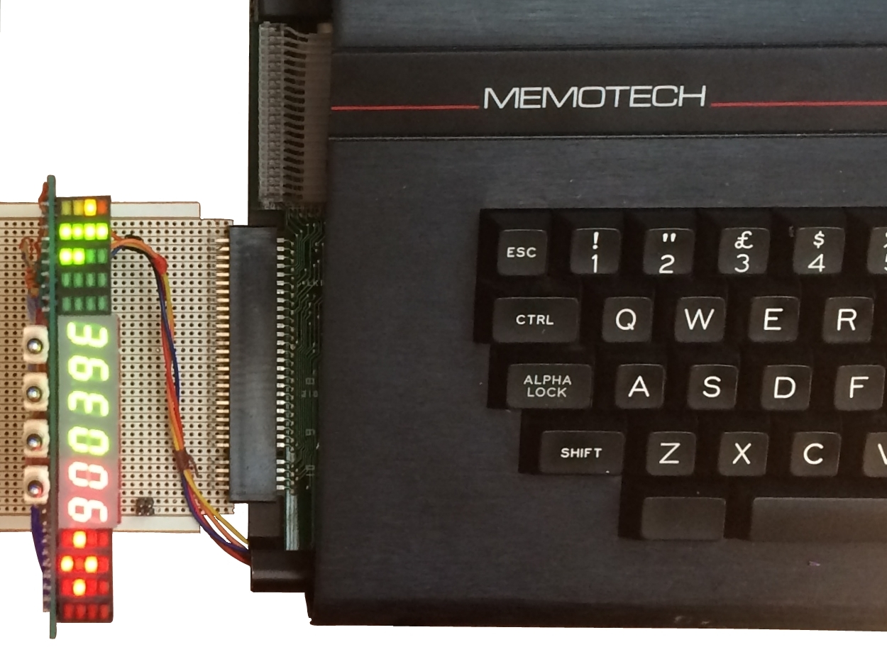
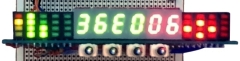
With the single step circuit
components fitted, and after correcting a silly
wiring error, the single instruction step
circuit appears to be working.
This photo was taken with an
MTX512 switched to single step mode, at this
point, the
WAIT,
MREQ,
RD
and INT
signals are all low. Having
looked at the MTX ROM disassembly, Martin was
able to advise that the CPU was stopped in the
middle of the keyboard scanning routine, 36DF
happens to be IN 6 and it’s pointing at the 6. |
 |
|
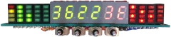
A slightly better photo, with
similar results Again, Martin has
advised that the display corresponds to the
start of the keyboard reading routine, 3622 3E
is the first byte of LD A,251 (I
really do need to learn to navigate my way
around the ROM listing) |
 |
|
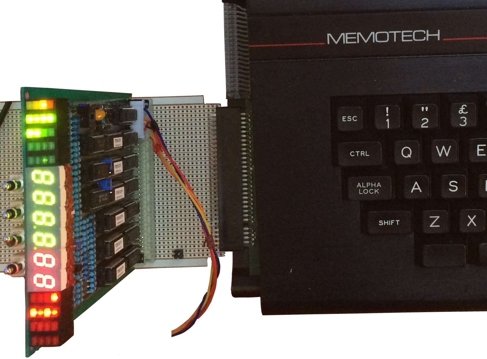
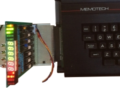
MTX Diagnostic Adapter |
|
Martin built one to help him
diagnose a problem with an ailing MTX and I
thought that it was a good idea to build one
too. The board only patches the signals from the
MTX cartridge port to the MTXPlus backplane
layout. Using the board on a good MTX will help
me get an idea of what the bus signals should
look like for an operating Z80 before I get to
testing the MTXPlus CPU board. |
|
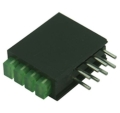
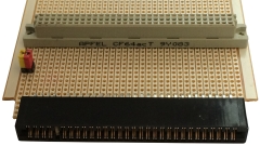
Slightly less impressive than
the diagnostic board - the MTX adapter.
The two jumpers allow me to
isolate the +5V and +12V lines on the MTX bus
from the diagnostic board. |
 |
|
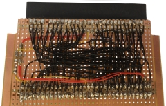
The wiring side of the board -
as you can see, the board just cross wires the
terminals from the MTX cartridge port to the
corresponding pins on the MTXPlus bus. |
 |
|
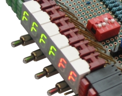
A rather blurry photo of the
board running on my original MTX512.
I hadn't fitted the single
instruction step components at this point (they
were on
order), so the 7-segment displays are showing
flickering "8"s as all of the segments are lit
displaying values at high speed. Similarly, the
LEDs are also flickering, but the indications
are consistent with what I expected, but are more
easily seen if I halt the CPU. |
 |
Limitations It is
recognised that many of the signals on the bus will
change state at relatively high frequency, even at the
4MHz clock frequency of the MTX computer, many of the
LEDs and the address & data values will rapidly change
state and may only be meaningful when the CPU is in
HALT or
WAIT states. To
mitigate that possibility, I now plan to include a very
low speed clock on the CPU card - in the order of 2Hz -
yes, that is Hertz! At that speed, it should be possible to
make sense of the changing control signals.
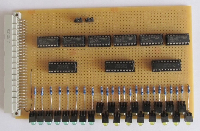
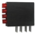
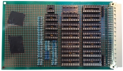
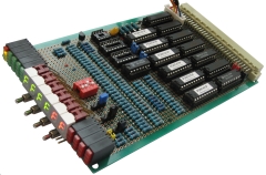
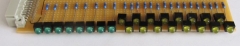
Martin's Diagnostic Board
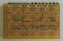
|
The component layout for
Martin's diagnostic board (prior to wiring)
To reduce the current
consumption, Martin has 6, manually switched
multiplexers, driving the 3 buffers and 24 LEDs. |
 |
|
A close up view of the LEDs,
which are all visible from the top edge of the
board |
 |
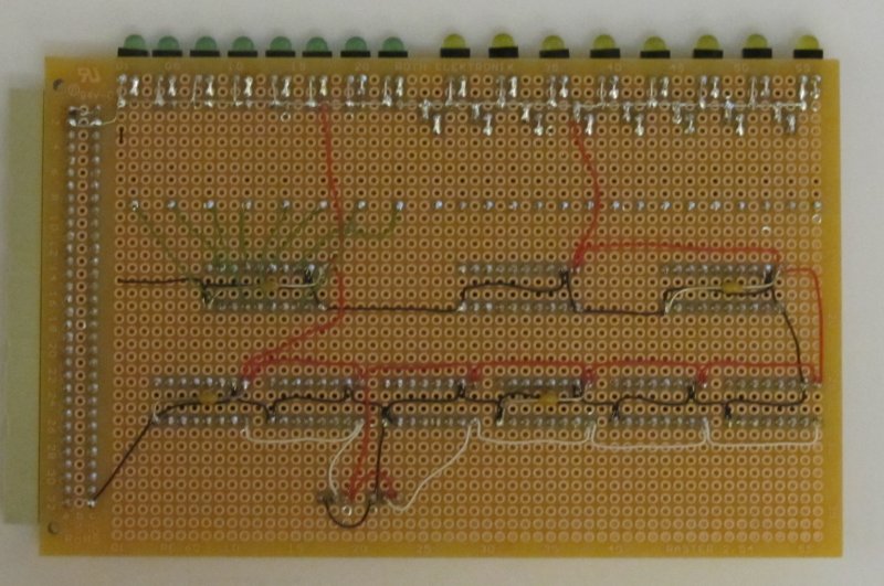
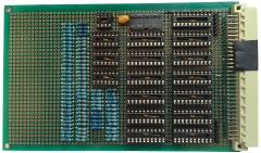
|
The wiring side of Martin's
board, at a very early stage of construction. |
 |
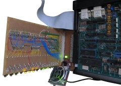
|
Using a simple adapter board,
Martin's MTXPlus diagnostic board connected to a
problematic MTX. |
 |
|