|
"MTX Plus+" -
Design Notes
Introduction
When I started out on this adventure, I knew that there were
a lot of holes in my (very limited) knowledge that were going to
need filling if I was to be able to bring the project to a
successful conclusion. I have been doing a lot of reading, but I
have been finding that there are occasions where a few words
from someone "in the know" can explain something that I struggle
to understand from books or web searches. This empirical
knowledge is probably already documented in books and other
websites, but for my own benefit, I have decided to capture
these significant "words of wisdom" on this page for future
reference.
There is likely to be little structure to this page and may
be nothing more than a few disjointed notes, but for what it's
worth - here it is!
| Date |
Topic |
By |
|
27/10/13 |
Trying to understand the function
of the VDP interrupt output (/VDPINT) function used
in the MTX, connected to CTC input 0. |
|
|
28/10/13 |
The Z80 CTC (Counter
Timer Circuit) is an interrupt controller as well as
a four-channel counter or timer.
When /VDPINT goes low at the end
of the last active display line*, the desired action
is to interrupt the Z80 as soon as possible. The CTC
achieves this by decrementing the channel 0
down-counter on the falling edge of its clock input
pin (connected to /VDPINT) and when the down-counter
becomes zero the CTC pulls /INT low and provides the
Z80 with an interrupt vector during the subsequent
interrupt acknowledge cycle.
In order that every VDP interrupt
generates a Z80 interrupt the down-counter is
programmed with the value 1, which is re-loaded into
the counter automatically when it reaches zero. At
the same time the channel 0 output goes high, so is
in effect the inverse of /VDPINT with a short time
lag. This output is not needed for anything, which
is why the pin is unconnected.
Due to pin limitations, channel 3
has no output and could have been used for /VDPINT
but channel 0 was chosen instead as it has the
highest priority.
* In contrast the ZX Spectrum ULA
does not generate an interrupt until the start of
the vertical sync, wasting a considerable time (over
3.5 milliseconds) that could been spent refreshing
the screen "invisibly" and without memory
contention. |
TB |
| |
The
question also generated some useful information on
the functionality of the CTC for use with the RS232
serial ports and the Z80DART
All 4 channels can count 4MHz clock
ticks (timer mode) or their channel specific input
(ch0=VDP, ch1 & 2=4MHz/13, ch3=cassette). Then reach
zero, channel output triggers (ch1/2 feed DART).
This is the reason the clock is divided by 13 by an
IC on the motherboard - so that it can be fed into
the CTC and divided to make all the various baud
rates, to then drive the DART. |
AK |
| 11/11/13 |
Trying to understand Memotech's
modifications to the MTX computer board for the
MTX512S2, i.e., the changes required to support
256KB of memory |
|
| 01/03/13 |
The specification of the original
MTX was a very close match to MSX computers, the
main differences being the Video Display Processor
and the Complex Sound Generator. As the MTXPlus
design develops, there may be an opportunity to add
MSX compatibility too. |
|
| 08/03/14 |
The
original intent was to use a 20MHz Z80 clocked at
full speed, but will now be 16MHz.
Martin identified a potential issue
with having a 20MHz system clock. "At 20 MHz the
cycle time is 50ns, allowing a cycle and a half for
a read/write gives 75ns to play with. Most Flash
Chips are 70ns, as is the RAM in
Lez's kit of
Z80 parts. That doesn’t allow enough time for the
chip select logic. The CPLD needs at least 15ns. At
16 MHz there’s some room to play with. The cycle
time increases to 62 ns, and read/write stretches to
93ns. 15ns for the CPLD leaves 78ns for the memory.
That’s then in theory plenty for 70ns ram and or
flash. 16 MHz might make the clock circuit more
versatile too.?"
Taking Martin's points on board, the
clock speed will now be 16MHz with additional 8MHz
and 4MHz rates. |
MA |
| 19/03/14 |
Giving some further thought as to whether a
degree of MSX compatibility is possible too,
investigating the potential hardware and I/O address
issues, see
this page for the status of my I/O port study. |
DS |
| 08/04/14 |
Mark Kinsey offered some tips on
power supply capacitors which I have taken on board
Also I remember reading that you
intend to use 4.7uF electro's for "bulk" decoupling.
I now use 10uF around boards, and a 100uF right next
to the power input pins, plus another 100uF (or
47uF) at the end of the power traces (the opposite
end to the power input). Always have a 100nF in
parallel with the electro's. |
MK |
| 11/04/14 |
Bus power considerations
The default configuration for the
backplane that I am using provides separate pairs of
power and ground planes, suitable for dual voltage
systems. These planes allow current to be supplied
to the cards in any slot via the pins directly
connected to the power (2 & 31) and ground (1 & 32)
planes. Although it is possible to cut a track on
the backplane and assign one of the ground planes to
a third power rail, the third power rail (+12V) in
MTXPlus has been assigned to pin 17c of the
backplane connector. Although the number of cards
that may require +12V is likely to be very small, to
reduce the potential to overload this trace on the
backplane, power to these pins will be connected by
wire wrapping to pin 17c of the individual slot(s).
The wire that I intend to use has a
maximum current rating of 400mA so this will be the
limiting factor on the 12V supply to each card slot.
It is likely that I will install suitable fuses on
the 12V line for cards that use the 12V supply. |
DS |
| 23/04/2014 |
Diagnostic Board : Single Step
Instruction Circuit In a "late design change", I
included the single step instruction circuit that I
had seen on the
Z80
Computer Project blog. This is a modified
version of the circuit included in Steve Ciarcia's
“Build Your Own Z80 Computer”, I could not find
contact details for the author on the blog page, so
hopefully, he does not mind me posting a copy of the
circuit description here - the original source of
thus information can be found on the
Single Step Instruction Circuit page on the blog.
"While debugging you may find you
would like to step through each instruction executed
to assure that the function of your system is
correct. Instead of cycling the clock over and over
to get through each instruction with a single-step
clock circuit, a new circuit can be built to receive
a de-bounced button press, and then execute one
instruction at the speed the Z80 is set to run at.
This requires a single-step instruction circuit. To
build such a circuit we will be exploiting two
control signals on the Z80, WAIT (Pin 24) and M1
(Pin 27).
M1 is an output control signal
that goes low each time an instruction is fetched.
WAIT is an input control signal that is sampled a
short time after the instruction fetch, and when
activated suspends the operation of the Z80. To
allow only one instruction to execute at a time a
D-flip-flop and one-shot are used. First, two NAND
gates (74LS00) are used to de-bounce a momentary
SPDT push button. The button press signal activates
the D-flip-flop (74LS74) triggering the WAIT line to
become high, and the Z80 to leave the WAIT condition
to run an instruction. After this instruction is run
the one-shot is triggered by the next M1 signal
which is prompted by the instruction fetch. The
one-shot’s output resets the D-flip-flop back which
activates the WAIT signal to pause the Z80′s
operation. The final toggle button adds a NAND gate
and a toggle switch for toggling between an
instruction stepping mode, and standard running
mode. The finished single-step instruction circuit
can be seen below. This circuit is a modified
version of the circuit outlined in Figure 4.5 of
“Build Your Own Z80 Computer” by Steve Ciarcia which
I also display below. Instead of using the 74LS121
as a monostable multivibrator (one-shot) I have
opted to use the 555 timer to cut down on the amount
of different parts needed. Also, I opt for 10K
resistors instead of 4.7K to standardize the
components needed."
Circuit Diagram
(on the Z80 Computer Project blog) |
DS |
| 09/05/14 |
Diagnostic Board : 7-Segment display drivers
The
Paladin Semiconductor PDN747, 7-segment display
drivers have now arrived but initially caused me a
bit of difficulty when I tested one on breadboard. I
could not get any output on the display and the
segment output ports were all stuck at logic "1". I
made a number of attempts to get some technical
support for the chip but Paladin seems to be a tiny
company with inadequate resources - that became
obvious after I placed the order, and despite a
number of promises of imminent shipment, the parts
took almost 7 weeks to arrive.
When I was trying to expedite
shipment of the parts, I discovered that the chip is
actually a custom programmed standard logic chip.
When I could not get any support from Paladin,
I lifted the label on one of the ICs to see if I
could identify the host chip and found that it was
an Atmel PLD, an
ATF16V8.
The Atmel datasheet revealed an
interesting discrepancy with the Paladin datasheet -
pin 11 on the Paladin datasheet is labelled "/BI"
and described as "blanking input". I
interpreted this to mean that this active low
pin would blank the display so had tied it
high for testing. The Atmel datasheet
labels pin 11 as "I9/OE",
in registered mode, pin 11 is output enable, i.e.,
must be low to enable the outputs.
Changing pin 11 from being forced high to being low
"magically" turned on the LEDs.
At this point, I discovered
another problem, the display would only update
following a "0" to "1"
change on pin 1 - the latch input. I had expected
that the latch would be required to "freeze" the
display, but when not set, the display would reflect
the status of the inputs. Again, the Atmel datasheet
proved useful, in registered mode, pin 1 is the
clock input and I will need to implement additional
logic to control update to the 7-segment displays. |
DS |
| 24/05/14
Updated
06/12/14 |
Diagnostic Board : 7-Segment display
latch input I have implemented a
number of options to trigger the 7-segment display
driver latches, selectable by the DIP switches
behind the displays :-
- System Clock (PHI)
- M1 - suggested by Martin.
"Could you drive the address latches with M1,
looking at the Z80 user manual It’s low during
the first 2 cycles of the opcode fetch, your
address indicators would then follow the program
counter, but ignore address bus changes involved
with load store. It also goes low on an
interrupt acknowledge cycle too, but then would
get re-activated on the next instruction fetch
anyway.
- Manually - mainly for initial
testing, but the display blanking switch also
has a momentary position, I use that to pulse
the display latches
- Logic driven signal from the
backplane (DIAG). During testing of the CPU
board, it was useful to have the CPU board CPLD
drive the latch for the 7-segment displays.
Although this could have been achieved using a
patch wire between the two boards, it does
provide additional flexibility for triggering
the displays, so it has now been added as a
backplane signal.
|
DS |
| 26/05/14 |
Diagnostic Board : Display blanking
circuit (TTL pull-down problem)
Whilst testing the diagnostic board, I came across a
very troublesome problem - with more than one or two
buffer chips installed, the enable lines for the
buffers and display drivers were sitting at 1.4V -
the range for TTL 0 volt rails is 0 to 0.8 volts so
the enable pins were being interpreted as being
high, disabling the buffer outputs and blanking the
LEDs.
To anyone who knows what they are
doing, the problem may have been obvious, but it was
not to me. I initially suspected that I had a bad
joint or partial short circuit somewhere, so I spent
a lot of time rechecking the connections and looking
for shorts.
In fact, the problem was not due
to bad construction, but bad design! When I decided
to implement display blanking, I wanted to be able
to set the enable pins for the buffers and display
drivers high using a toggle switch, or to be pulled
low by default. I thought that the easiest way was
to daisy chain all of the enable inputs together and
switch them in one.
This is the relevant section from
the diagnostic board schematic, the "BLANK" signal
is connected to pin 6 of the PDN747 display drivers
and pins 1 & 19 of the 74LS24x buffers, the display
drivers are CMOS devices and the buffers are TTL.
I wanted to minimise
the power consumption and so wanted a "weak
pull-down", i.e., to use a high value resistor. What
I had failed to realise is that TTL inputs are
actually current sinking, an LS TTL input needs to
be able to sink 0.4mA to be interpreted as a logic
low. The voltage drop across a pull down resistor
needs to be no more than 0.8 volts to meet the TTL
specification of 0 to 0.8 volts for a low level. (CMOS
devices can operate with much higher pull resistor
values and were not a problem here). Pull up
resistors are less of an issue due to the wider
margin of voltage levels for a high input signal of
2 to 5v.
So, for the 74LS24x buffers,
as each has two enable pins, there are 14 TTL inputs
that need to sink current to 0v, using Ohms law :
| R = V
/ I |
where |
V = a maximum of 0.8
volts |
|
| |
|
I = total current, 14
* 0.4, or 5.6 mA |
|
|
Rmax |
= |
0.8 / 5.6 e-3 |
|
| |
= |
143 ohms |
|
This is significantly less than
the 10k resistor that I had used and also the 4.7k
value frequently used for pull-ups. Using the
formula above, it can be seen that a single LS TTL
gate would could be pulled to 0.8V with a 2k resistor,
but my 10k for 14 (or more) inputs was well wide of
the mark. When I was looking for a suitable
replacement value for the resistor, I was initially
worried about the power requirement, so, I tried
reducing the 10k value by "trial and error" to find
a suitable value that would draw the minimum amount
of current and found that a 1.3k resistor seemed to
work.
Update : When I built an adapter
to allow the board to be used with a standard MTX, I
found that the elevated voltage on the enable pins
caused some problems, including the displays failing
to recover from being blanked, so I decided to
replace the pull-down with the correct value. The
closest standard resistor value less than 143 ohms
is a 130R which would result in "wasted" power of
about 38mA but this is fed from the 5v line that
only powers the display drivers, but not the
displays themselves, so that will not be a problem.
It does illustrate why TTL pull-downs are not
recommended - they use a lot of power.
After replacing the resistor, the
intermittent display problems etc. went away.. |
DS |
| 07/06/14 |
CPU Board -
Real Time Clock
The kit of parts
that we received from Lez included a Dallas
DS12887 RTC, this is a "drop–in" replacement for
the IBM AT computer clock / calendar, it is
compatible with the Motorola
MC146818B used by IBM and the compatible Dallas
DS1287. The DS12887 self–contained subsystem and
includes lithium battery, quartz crystal, support
circuitry and an expanded area of 114 bytes of
general purpose non-volatile static RAM (NVSRAM).
There are not many examples on the
web of the use of this RTC on a Z80, but I did find
this really
helpful article written by a Wilf Rigter around
1996. The article demonstrates the use of the DS1287
with a ZX81 and included examples of Z80 assembler
and BASIC programs to access the chip.
Martin was able to use this
information with the DS12887 and modified address
decode logic to make a working RTC that will be
included on the MTXPlus+ CPU board.
Martin has posted the details on the
Memotech forum in this thread |
DS/MA |
| 14/06/14 |
Video Board
- Video Output
With the Yamaha V99x8 being used in the later models
in the MSX range (MSX 2, 2+ and Turbo R), there are
copies of OEM service manuals available on the web
that show how the VDP was implemented. As you would
expect, the input side of the circuits are pretty
consistent, i.e., the CPU interface, clock
generation and VRAM interface.
However, there is much more
variation on how the RGB outputs were conditioned
for the TV/monitor, some designs used transistor
circuits to amplify the RGB outputs and other
systems used a Sony
CXA1145 RGB Encoder
to generate a composite
and/or component output as well as the RGB. The Sony
chip is obsolete and the only datasheet that I can
find has very little English in it, the
ES71145 is functionally equivalent and has an
English datasheet available.
It appears that just about every
MSX manufacturer had a different implementation of
the video output circuitry, particularly when using
the CXA1145 where the values used to implement the
required band-pass filter varied widely.
The easiest solution to implement
appears to be an RGB only output, but I would also
like to have a composite video output available. To
allow the video board to support two versions of the
video output circuit, the board will have pin
headers to allow an appropriate daughter board to be
connected - very much like the design of the
original MTX video board. The daughter board will
also provide other headers for the TV/monitor audio
and video output options. We felt that using a header rather than
mounting the SCART socket or other connectors
directly on the video or daughter board would put
less strain on the board and provide more
flexibility in use.
The other advantage of having the
output components on a daughter board allows us to
design and build the base video board while we
finalise the output configuration and should enable
easier "tuning" of the output side of the video
board if required.
Some comments on the CXA1145 on
this (non-MTX) thread |
|
| 21/06/14 |
Video Board
- Video Output Update Still
struggling somewhat to find a suitable circuit
design for the output side of the video board, I
came across the
GR8BIT project. GR8BIT is a Z80 based hardware
and software project, supplied as a self-assembly
kit, based on an ATX type motherboard and a bus
architecture, with additional boards providing, CPU,
Memory, Video functions etc. that plug into the
system bus. (full
specifications).
GR8BIT is capable of running MSX2
software and uses a Yamaha V9938. I was very
interested in how GR8BIT had implemented the V9938
design and contacted the designer, Eugeny Brychkov.
Eugeny was very helpful, pointing me to the video
board design on the Yamaha YIS503 MSX2 machine and
also the
GR8BIT Knowledge Base article on adding
Composite and S-Video output (KB0014).
In addition to the RGB output, I
intended to include a component or composite video
output and, being in the UK, I had planned on making
the output meet the
PAL
standard rather than
NTSC.
However, during our discussion, Eugeny pointed out
that most modern TVs can accept both PAL and NTSC
signals. The VDP has an NTSC compatible clock output
available (3.58 MHz) but a PAL sub-carrier clock
(4.43 MHz) would require an external crystal
oscillator and associated circuit. To make things
easier, the video output from MTXPlus+ will now be
NTSC, this may give problems with older TV's, but a
PAL compatible output could be added later if
required. Other learning's
for this week include a better understanding of the
differences between the VDP composite sync pin
between the V9938 and V9958. On the V9938. the CSYNC
line on Pin 6 is a tri-level logic I/O pin : High
for composite sync output and Low for VSYNC input.
To use the CSYNC output with a V9938, the tri-level
logic signal has to be converted to a 2-state
signal. This is not required on the V9958 where Pin
6 is composite sync output only, this helps explains
the differences between the CSYNC circuits between
the MSX machines using the different processors. |
DS/EB |
| 24/06/14 |
Video Board
- Video Output Update 2
Although the
V9958 will run V9938 software, the are some minor
hardware differences between the two VDPs which
means that some parts of the V9938 VDP output
circuit design need to be modified to work on the
V9958, for example, the CSYNC signal described
above. Notwithstanding Eugeny's help with the V9938
circuit, I continued to look for examples of
implementations of the V9958 by MSX manufacturers.
Having been used in various
MSX2
machines, there are quite a few, albeit different,
designs using the V9938. The V9958 were used in a
smaller range of
MSX 2+
machines manufactured by Panasonic (FS-A1FX,
FS-A1WSX, FS-A1WX), Sanyo (WAVY PHC-70FD, WAVY
PHC-70FD2, WAVY PHC-35J) and Sony (HB-F1XDJ, HB-F1XV
), the last machines in the MSX range were the
Turbo
R computers, only manufactured by Panasonic as
models FS-A1ST and FS-A1GT. MSX 2+ and Turbo R
machines were only produced for the Japanese market,
so the few circuit diagrams that are available are
in the Japanese MSX service manuals.
I have not been able to locate
service manuals or schematics for any of the Sanyo
or Sony MSX2+ machines, but Hans Otten's
MSX Info Pages has copies of the Panasonic
FS-A1FX circuit diagrams and the full service
manuals for the FS-A1ST and FS-A1GT. These circuit
diagrams will form the basis of the "digital" video
card daughter board, using a slightly more modern
version of the Sony CXA1145P, the
CXA1645P to output
RGB, Composite and S-Video. As Martin is
uncomfortable using the very old Sony parts, the
"analogue" daughter board will be based on the
MSX2/V9938 design, using transistors to amplify the VDP RGB outputs.
|
DS |
| 04/09/14 |
Video Board - "Lesson Learned" about Tantalum
Bead Capacitors ! Write up to
follow - quick version - don't get the polarity
wrong :-)
See this video to get the idea though
|
DS |
| 03/10/14 |
Video Board
- Minor hold up in testing With the
Video board built and the Daughter Board fitted, I
had a bit of a setback. I was unable to get a
picture from the V9958, and even worse, with the
Video board connected, the MTX now had problems - it
would boot OK, but had various issues, including
corrupted display, random freezes and crashes to
PANEL.
Removing the DB and all of the ICs
on the video board, the problem was seen to occur
once the GAL was installed. I initially suspected
that I had created the problem by breaking or
shorting a connection on the wire side of the board
as I messed with the DB. Having retested the board
with a meter and not finding any faults, I tried
disconnecting the pins of the GAL (using an
interposing spare socket between the socket on the
board and the GAL and bending the legs out of the
way) in groups, starting with the outputs then the
Z80 control signals. To my surprise, I found that
the problem was being caused by the /M1 line,
although the GAL verified correctly on the
programmer, it caused the problems described.
Replacing the GAL has fixed the problem. |
DS |
| 30/10/14 |
Video Board
- SCART Connection
| Martin got to the stage of testing
the video board SCART outputs before I
did and found that the composite video
output was not working when connected
via the SCART connector.
We were not
aware that SCART cables have cross-overs
in the connections for audio and
composite video. Making the cross-over
between pins 19 and 20 in the SCART
connection allowed the composite video
signal to be displayed on the TV. |
 |
| |
Image downloaded from
leadsdirec.co.uk |
|
MA |
| 15/11/14 |
CPU
Board - Processor Issues
Once
again, Martin got to testing the CPU board before I
did and found that he could not get the Z84C0020PEC
CPU to work above 10MHz. Having tried a second CPU
and having been able to run a known good 10MHz chip
reliably at over 20MHz, we suspected that the
"20MHz" were not what they purported to be.
I have made a few
notes on counterfeit
chips on a separate page, but in summary, based
on some limited testing and close inspection of the
chips, we believe that the "Z84C0020PEC" CPUs are
actually remarked Z80H (8 MHz NMOS) rather than
20MHz CMOS, so we will need to source replacements
if we are to run the CPU at 16MHz.
|
As described on the
counterfeit
chips page, I did a bit of "Googling"
and found a method of determining
programmatically whether a Z80 was an
NMOS or CMOS version.
On an NMOS Z80, an OUT
(C),0 instruction outputs 0, on a CMOS
Z80, OUT (C),0 outputs FFh. Martin used
this information to run tests on a
number of Z80 CPUs that he had to hand,
which gave the results shown
|
 |
|
DS/MA |
| 20/11/14 |
CPU
Board - Data Bus Issues
During testing of the CPU board, it
became apparent that there was a problem with the
74HC245 buffer that I had installed between the
on-board data bus and the backplane. Tony Brewer was
quickly able to pin-point the problem with the way
that I had configured the data buffer.
In my original design for the CPU
board, based on references such as Steve Ciarcia's “Build
Your Own Z80 Computer”, the address and data
buffers were configured on the outlet pins of the
Z80. Someone queried whether this position was
necessary, i.e., whether it was really necessary to
buffer the bus lines for the components installed on
the board. Not knowing the reason they were in that
position in the first place, I relocated the buffers
to the where they just buffered off-board access to
the bus lines. I was really just thinking about the
ability of the CPU to drive multiple devices on the
bus, but using CMOS devices, this is not likely to
have been a problem anyway.
Unfortunately, I had not understood
the effect that this would have, Tony advised that
the "A" side of the buffer should be connected to
the Z80 and nothing else. The "B" side of the buffer
should be connected to the memory on the CPU board
and the backplane. Tony explained that with the "B"
side of the buffer connected to the backplane only,
then there would be a conflict when the CPU was
trying to read ROM or RAM as the 74HC245 buffer
would also be driving the on-board data lines. Tony
also provided a useful reference to the
Tatung Einstein schematic.
In the short term, testing will
continue with the data buffer bypassed until I can
rework the CPU board to re-position it where it
should be.
Tony also advised that Buffer output
enables should be actively switched, rather than
just connected to ground. connected to +BUSACK (/BUSACK
inverted), not ground. /RD is much better than /WR for
direction control, but /RD by itself is not enough as
you need to cater for reading interrupt vectors if
the CTC is
on the B side of buffers.
On the subject of busses, the Z80
address bus is unidirectional, i.e., only the CPU
drives the address bus and direction is not really
meaningful. When an external device wants to take
control of the busses, it sets
BUSRQ
low to request the Z80 take the address bus, data
bus and tristate control outputs to the high
impedance state. When this is done, the CPU sets
BUSAK
low.
This is not an issue at the moment,
but should external devices, such as a DMA
controller be needed, the position of the address
buffers would be problematic as components on the
CPU board would become isolated from the address
bus.
|
TB |
| 25/11/14 |
I/O Board
- General
Printer Interface - Strobe line (Reference)
When the host transmits data to the
printer, it first places an eight-bit byte to be
sent on the DATA lines, DATA0 through DATA7. Once
those electrical levels are stable, the STROBE* line
goes LOW for 1.5 microseconds, plus or minus
500nsec. The printer is alerted to the presence of
new data when the STROBE* line goes LOW. |
DS |
| 26/11/14 |
CPU Board
- Real Time Clock We had intended
to use the Motorola bus timing mode for the RTC, but
have decided to change to the Intel mode instead, to
enable Intel mode, the MOT pin will
will now be tied to 0V, rather than 5V. For
flexibility, a jumper has been added to the board
design to enable selection of Motorola (+5V) or
Intel (0V) bus mode. |
DS |
| 30/11/14 |
I/O Board
- Serial Ports My original I/O
board design was based on the use of a Z80DART for
the serial ports, however, Martin questioned whether
the same situation would exist
as with the CTC,
i.e., that the DART had to be clocked at the same
rate as the CPU. In this case, the Zilog
documentation is a more explicit and says "“The Z80
DART uses the standard z80 single-phase system clock
to synchronise internal signals”.
Therefore the I/O board will now
use a CMOS Z84C4010 - as with the CTC, the fastest
available in a DIP package is 10MHz. |
MA/DS |
| 15/12/14 |
I/O Board
- IDE / Compact Flash interface An
82C55 Programmable Peripheral Interface (PPI) will
be used to provide an IDE interface to a Compact Flash
(CF) reader for non-volatile storage.
For 8 bit microcomputer like
MTXPlus+, a large hard disk would be overkill, and
even a relatively small Compact Flash card will
provide more than adequate storage for the system.
Compact Flash cards contain an embedded IDE/ATA
controller and can be interfaced in exactly the same
way as an IDE hard disk. CF card readers that
connect directly to an IDE interface cable are
readily available and cheap - Lez also included one
in the kits of parts that he provided.
The IDE
standard provides for both 8 and 16 bit data
transfers, as it is simpler to implement, a number
of "homebrew" IDE interfaces use 8 bit mode, but 16
bit mode will be used for MTXPlus+.
The IDE/CF interface will be based
on the
S-100 IDE Interface board found on the
S100
Computers website, but, due to space limitations
on the MTXPlus+ I/O board, will only feature a
single IDE/CF connector and a single status LED
(Activity). The intention is that the CF card will
be FAT compatible and can be written/read on a PC to
facilitate creation and editing of "disks".
The S100 site also makes available
the source code for a short diagnostic program (MYIDE.ASM)
written by the board designer. The source is in 8080
assembler, but was a lot easier for Martin to
translate to Z80 than the 8051 code that he had
seen.
This
text file, courtesy of Martin, is a copy of the
draft ANSI
standard for
IDE. |
DS/MA |
| 28/12/14 |
I/O Board
- JTAG Interface
The I/O board has two Altera EPM71xxS
CPLDs installed, these are "in-system" programmable
using a
JTAG interface. The two devices can be
multi-dropped and individually selected by the
programming software when required.
Although
I believe that the two devices will operate over
JTAG without issue, I think that it is usual to
install buffers for each device. Since board space
is at a premium, I have chosen not to install any
buffers, but each device can be
connected/disconnected to/from the JTAG lines using
jumpers on the front edge of the board. Initially,
both CPLDs will be connected to the bus, but if
problems are seen, then the devices can be
individually disconnected.
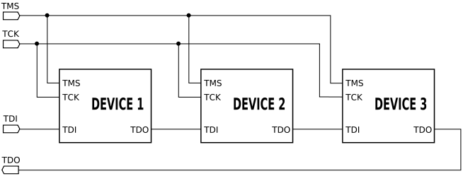
Wikipedia diagram
of diasy chaining JTAG devices TMS and
TCK are directly connected to all
devices. TDI and TDO pass through each
device in the chain.
| TDI |
Test Data In |
TDO |
Test Data Out |
| TCK |
Test Clock |
TMS |
Test Mode
Selct |
|
 |
|
DS |
| |
Video Board
- VDP Update Rate The original MTX computer using
the TMS9918A/29A had the VDP interrupt pin (INT)
connected to channel 0 of the Z80 CTC (named
VDPINT
on the MTX). The VDP generates an interrupt at the
end of each active display scan, which is about
every 1/50th of a second for the PAL version. |
DS |
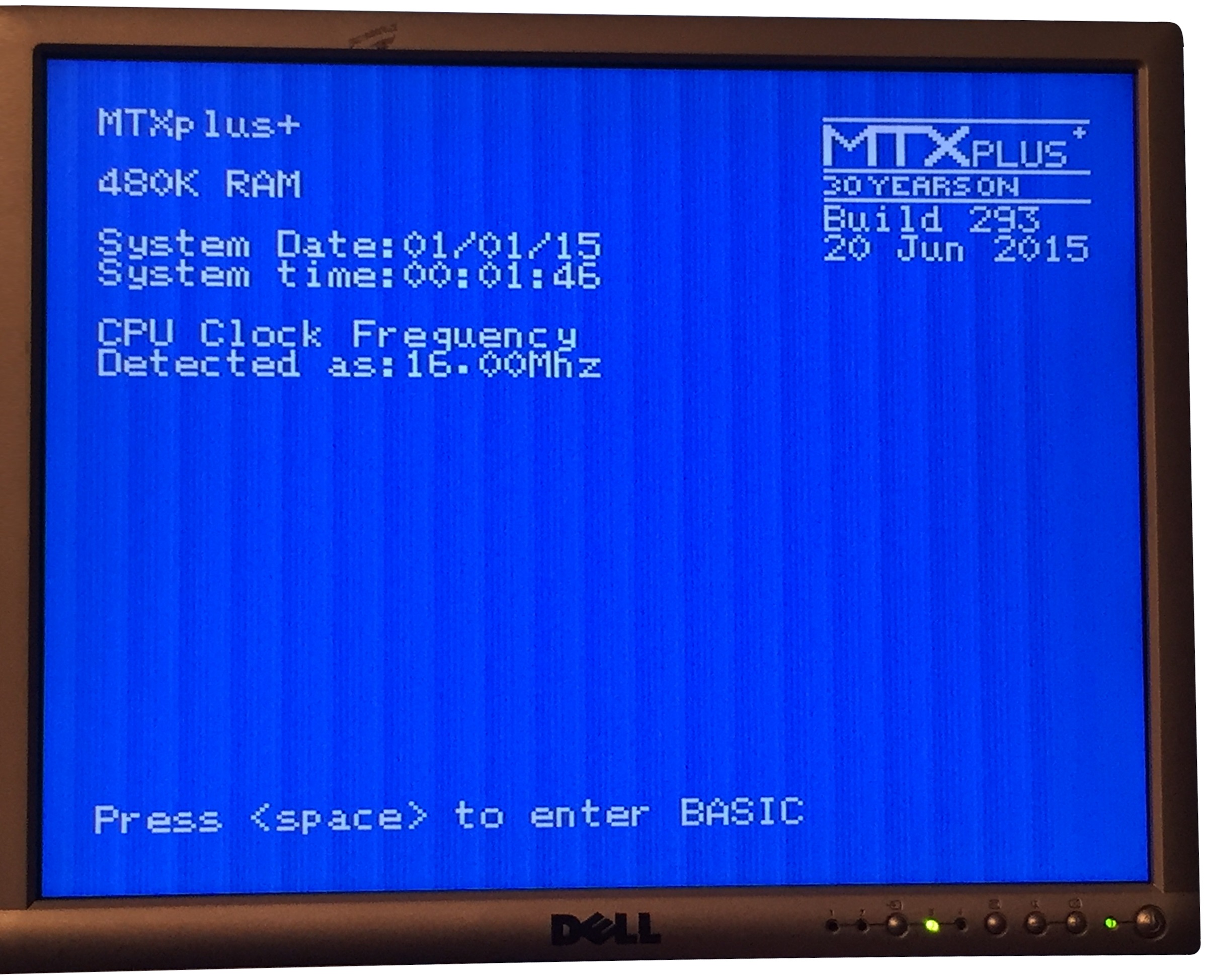
| 31/10/15 |
I/O Board
- Keyboard problem
When I got back to
investigating the video issues, I lost a few
hours with an annoying problem with the
keyboard that I think is worth a mention.
The keys at the very left of the keyboard
were behaving very oddly, they worked
perfectly at 4MHz, but misbehaved at faster
speeds, generating incorrect, but repeatable
codes. Replacing the keyboard had no effect
on the problem, nor did replacing the ICs on
the I/O board. |
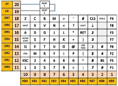
This diagram, from
my
MTX keyboard technical note, shows that
all of the affected keys are connected to
the KB0 sense line.
The wiring on my
I/O board is pretty congested and I
suspected that a bad solder joint or other
physical problem could be the cause, so I
spent quite a while checking and remaking
connections on the KB0 sense line. When that
did not reveal a problem, I did the same for
data line D0, which is used to read the KB0
sense line. |
 |
The D0 connections on the
board also proved to be fine. The only
remaining component was the keyboard
interconnect cable. The cable that I had
been using was a brand-new, 40-pin IDE
cable, supplied by HP and still in it's
sealed packaging when I started to use it. I
did not have an equivalent cable easily to
hand, but when I managed to dig out another
cable, the problem was fixed!
I still
find it surprising that a "bad" cable could
work without fault at 4MHz, but fail at
faster speeds, but that was the case. The
time taken to find & fix the problem was
exacerbated by not having another cable
available - aaaarghhhh! |
|
DS |
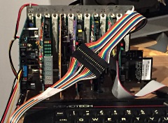
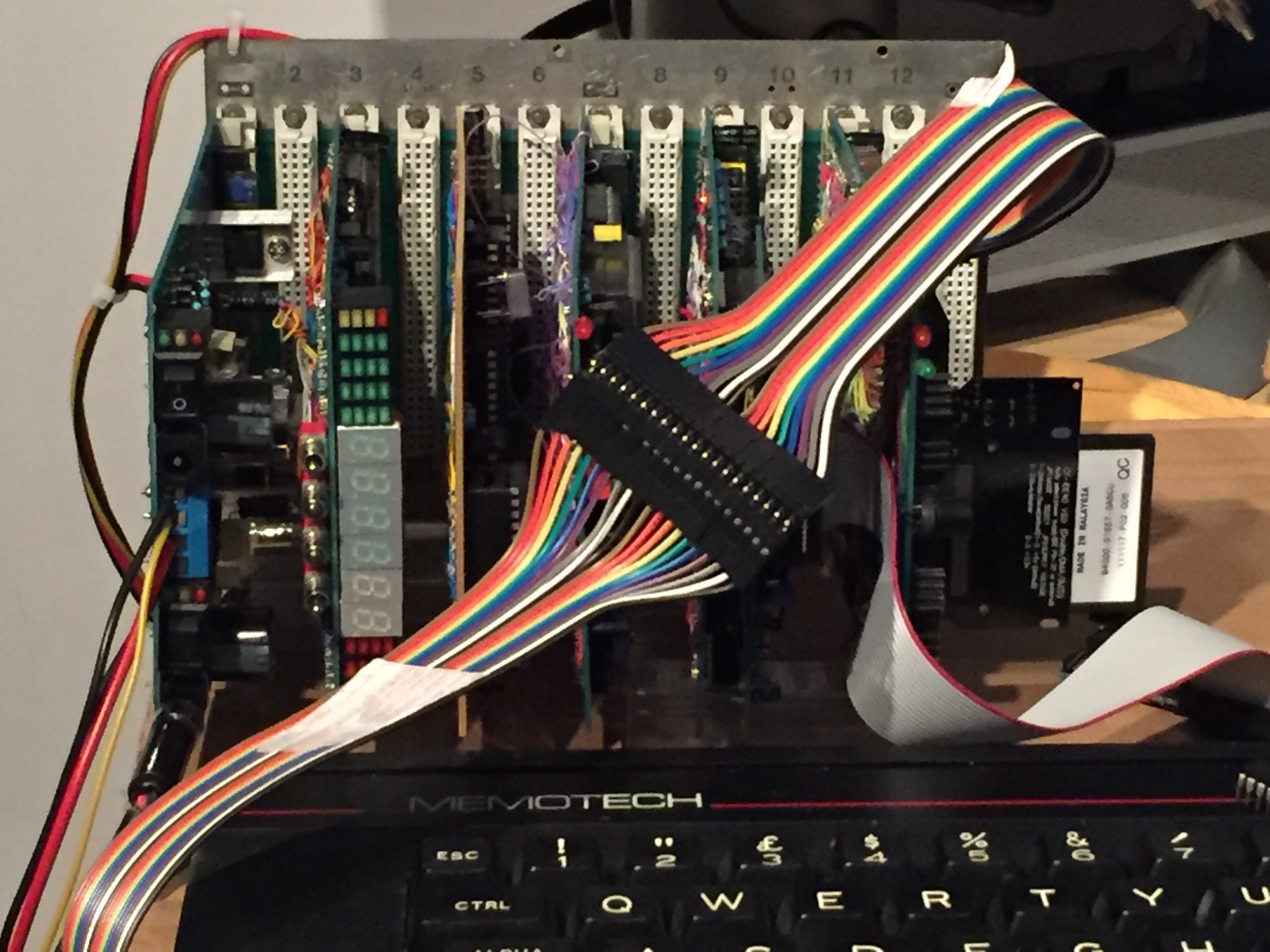
| 30/12/15 |
Backplane Issues
I had been experiencing
issues with the stability of the system for some
time, at faster CPU speeds, the system was very
sensitive to the position and spacing of the boards
on my backplane, an issue I put down to the lack of
proper termination on the bus. I had been
considering trying to build a couple of bus
terminator boards to put at either end of the
minimum number of slots required to install the
boards, perhaps 13 backplane slots, allowing for the
required clearance between the boards.
I had
previously borrowed a reduced sized, hand wired,
backplane from Martin and had not seen the issues
when running with a smaller bus so I was pretty
confident that the issues were bus related. However,
I was not confident in my ability to design proper
bus terminators and decided on a more radical,
perhaps even reckless, course of action . . . . .
Cue the hacksaw !
What you see here is the new, "cut-down"
(literally), MTXPlus+ system backplane with
13 slots and 6 boards installed.
Limited testing has shown that it has not
had any adverse effects and it does appear
to have helped the system's stability, at
least up to 12Mz. |
 |
|
DS |
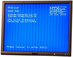
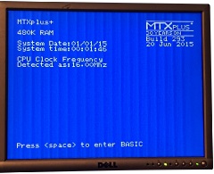
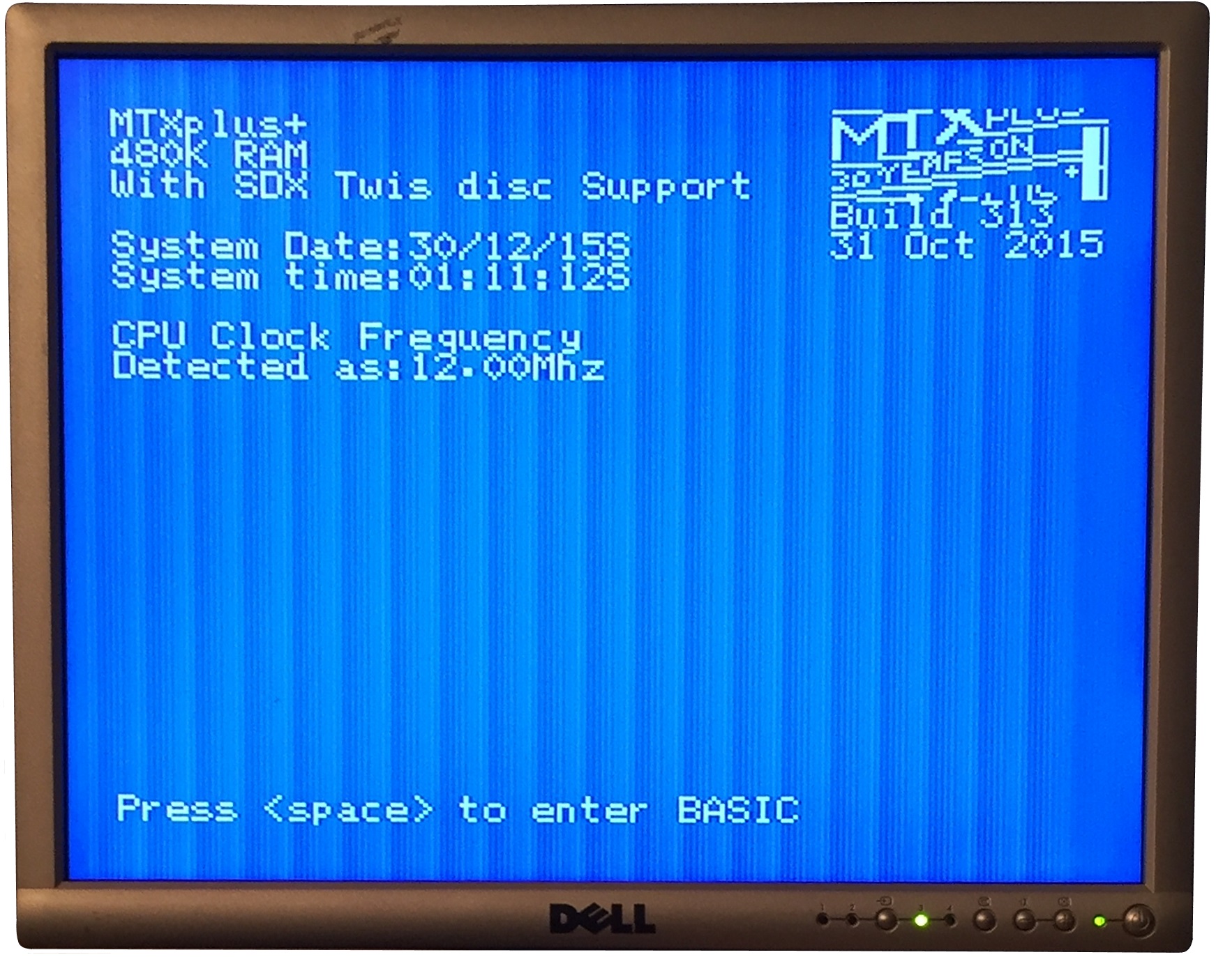
| 31/12/15 |
The CPU runs quite
happily at 12MHz, but you can see some video
corruption in this photo.
This is
the MTXPlus+ "Duo" ROM mono CP/M
system, booting in 40 column mode, with the
VDP writes being slowed using the CPU WAIT
signal.
The system booted CP/M
without issue, but also showed display
corruption at this speed.
|
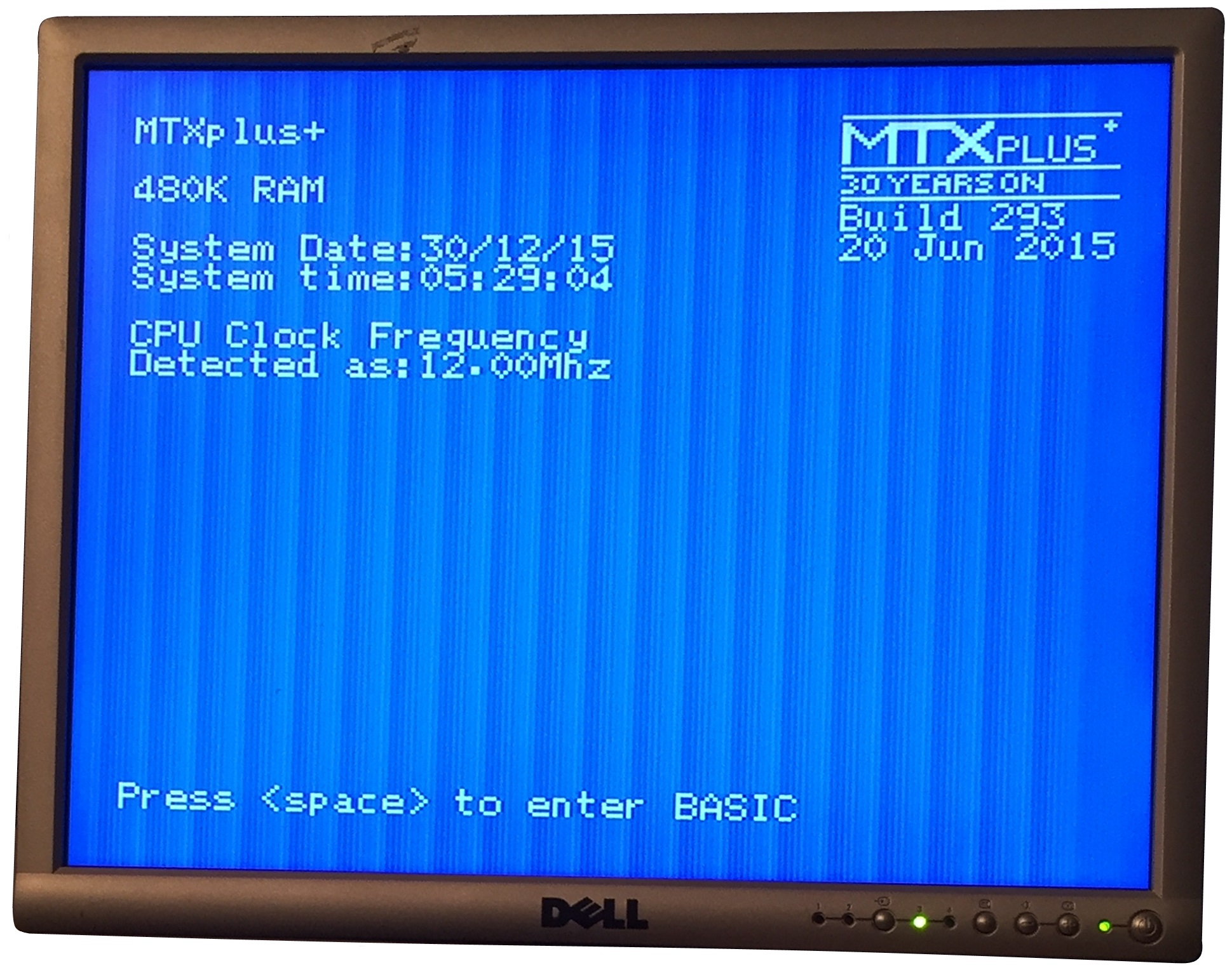
 |
Also at 12MHz, this
is the "Duo" ROM colour CP/M
system, booting in 40 column mode. This ROM
also inserts software waits that are good
for up to 20 MHz.
Note the lack of
corruption to the video display that was
seen in the previous image. |
 |
With the same
configuration, the system boots happily at
16MHz and has uncorrupted video display.
However, the system will not boot CP/M,
some video corruption is present on the 80
column screen and the system can not "see"
the Compact Flash drive. |
 |
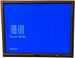
Although it is not
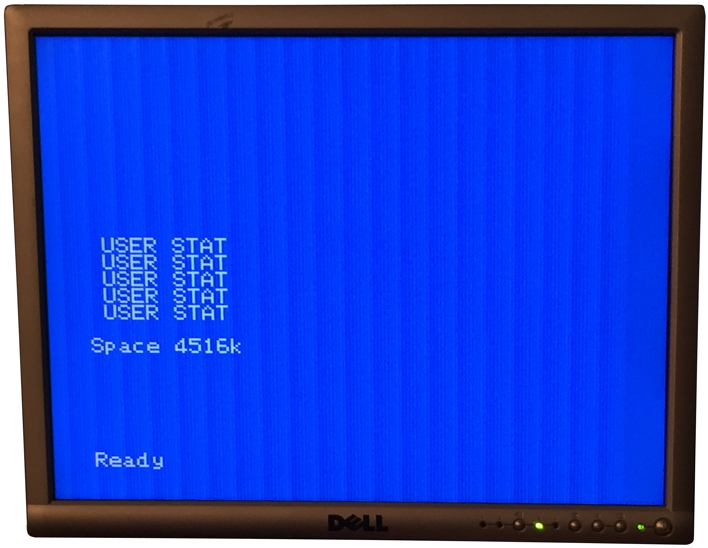
reliable, the CF drive occasionally responds
to commands from BASIC, in this example, after 5
attempts, the system responds to the
STAT command.
The
behavior of the CF drive was not consistent,
sometimes resulting in "BDOS Errors",
sometimes resulting in the system reporting
"No Line" in response to BASIC commands,
and, very occasionally, actually working. |
 |
Using different
82C55s from the same or alternative
manufacturers sometime produced different
effects, but on the whole, the behavior was
pretty haphazard.
|
 |
A selection of different
manufacturers 82C55s are shown in
the table. None of the chips have a
speed rating anywhere close to the
system clock speed of MTXPlus+, 8MHz
is the fastest 82C55 available, but
that is not necessarily an issue.
The key consideration is the
timing requirements given in the PIA
datasheets. The minimum Read and
Write pulse widths (in ns) are
shown. |
Manufacturer |
ID |
Speed |
Min
RD |
Min
WR |
|
Intersil |
CP82C55A-5 |
5MHz |
250 |
100 |
|
Intersil |
CP82C55A |
8MHz |
150 |
100 |
|
OKI |
M82C55A-5
|
5MHz |
300 |
300 |
| OKI |
M82C55A-2 |
8MHz |
100 |
150 |
| Intel |
8255A-5 |
5MHz |
300 |
300 |
| Intel
|
82C55A2 |
8MHz |
150 |
100 |
| Mitsubishi |
M5L8255AP-5 |
5MHz |
300 |
300 |
|
The Z80 timing diagrams show that
IORQ and RD/WR are valid for just
over 2 cycles, which translates to
the figures in this table. It can be
seen that the 5MHz PIAs are only
likely to work with a CPU clock
speed of < 8MHz and none of the
others are likely to work reliably
at 16 or 20MHz.
Using a PIA
with a minimum R/W speed of 150ns
would equate to a CPU clock speed of
~13.3MHz - this may be the limit for
MTXPlus+ using a 82C55A based disk
drive. |
CPU PHI
MHz |
Period
ns |
Z80 R/W
ns |
| 4 |
250 |
500 |
| 8 |
125 |
250 |
| 12 |
83 |
167 |
| 16 |
63 |
125 |
| 20 |
50 |
100 |
|
| |
|
| |
|
| |
|
| |
|
|
DS/MA |
| 24/01/16 |
CPU
Board - Clock speed reduced to 10MHz
Although the CPU operates quite
happily at 16MHz (and beyond), the system is
constrained by the maximum speed of the I/O and
peripherals. A lot of effort (with a great deal of
assistance from Tony) was put into getting the VDP
to operate above its rated speed by inserting
hardware wait states. Whilst the problem was not
completely resolved for speeds above 12MHz, other
constraints have emerged that mean that it's a moot
point anyway.
The I/O board uses an 82C55 PIA
to drive the Compact Flash reader, the 82C55 is only
available with a maximum speed rating of 8MHz (this
is not necessarily the system clock speed). At
speeds above, say, 12 MHz, operation of the CF
reader on MTXPlus+ has proved to be problematic. In
addition, the Z80CTC and SIO are only available in
speeds of up to 10MHz.
So, even though it has
been interesting to try and find ways to get the
MTXPlus+ prototypes to operate as fast as possible,
for a "production" version, it is more sensible to
stay within the specifications of the components,
therefore, the "nameplate" speed of MTXPlus+ is now
set at 10MHz. |
DS |
| |
|
|
| 21/08/18 |
PCB Design Notes
Like just about everything
else in the Project, the design of the MTXPlus+
PCBs is an area where I have little experience and,
to anyone with any knowledge of the subject at all,
there are likely to be any number of glaring errors
and basic design rules that I have ignored. Whilst I
have done some research and followed what I think
are good design practices, it is beyond doubt that
the boards could be better designed to reduce signal
"noise", crosstalk, etc. etc. FWIW, the fundamental
aspects that I have tried to consider are described
here.
Decoupling
The PCB designs include 0.1uF
decoupling capacitors for all of the ICs, I have
tried to locate these as close as possible to the
VCC and VSS pins at each IC.
Trace
Widths
I have used a default trace
width of 10
mils, this was the default setting in KiCAD and
critically, exceeds the minimum conductor width (>8
mils) specified by the PCB manufacturers that I use
(Itead Studio).
Obviously, a small conductor width makes routing
easier, but has less current capacity and a greater
voltage drop than a larger conductor.
The
thickness of the copper on a PCB is specified in the
weight of the copper in ounces - typically, 1oz
or 2oz. An interesting unit of measure for
thickness! The value is the resulting thickness if
the specified weight of copper were to be pressed
flat to occupy a space of 1 square foot - for 1oz of
copper, this would be 1.37mils. My PCB designs are
based on 1oz copper thickness.
KiCAD includes a
handy PCB calculator that helps determine
the impact of varying conductor size for a
given weight of copper. The user can specify
an acceptable temperature rise and conductor
length and the calculator reports the
maximum current carrying capacity and
voltage drop for the conductor.
For
the signal lines, I did not consider that
the default trace widths would have any
issues with current capacity or voltage
drop, but the power lines probably did need
special consideration. |
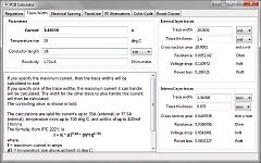 |
Since the MTXPlus+ PCBs are
Eurocard format (160mm x 100mm), I used 15cm as
an average estimate for conductor length and used a
permissible temperature rise setting of 10 Degrees
C. Although the maximum current carrying capacity of
the trace was a consideration, I chose the power
line trace width to ensure that the voltage drop
along the conductor length was no more than 0.2V.
The MAX705 microprocessor supervisory IC
generates a reset if the supply voltage drops below
4.65 volts, and I wanted to make sure that VCC
should not get anywhere near that on the PCBs. This
resulted in a trace width of 20 mils, which has a
current rating of ~1.5A - significantly more than
any of the PCBs require, so, it is over-specified
for the current requirement, but suitable for
limiting the voltage drop to my specification.
|
DS |
| |
|
|
| |
|
|
| |
|
|
Credits
| MA |
Martin Allcorn |
| EB |
Eugeny Brychkov |
| TB |
Tony Brewer |
| AK |
Andy Key |
| MK |
Mark Kinsey |
| |
|
| |
|
| |
|
| |
|
| |
|
| |
|
| |
|
|


