|
Hardware Design |
| System Bus Design Schematic (Version 1.02) |
 |
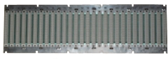
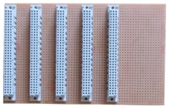
| The system will be based on a
Eurocard type backplane, with individual boards for the
major functions such as CPU & memory, video
processor & VRAM, I/O etc. I bought this used
backplane for £5.00 off ebay for development &
testing the concept, the finished system will
require a much smaller bus - even allowing for
expansion, probably 6 slots at most. |
 |
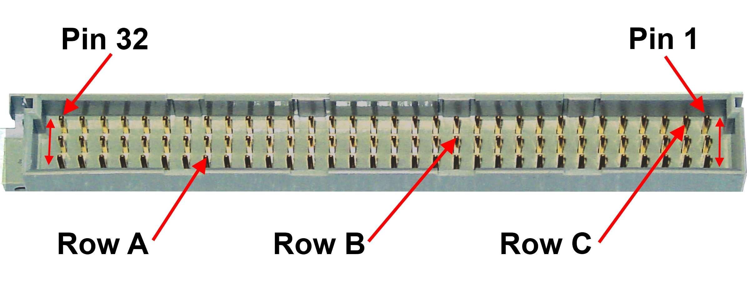
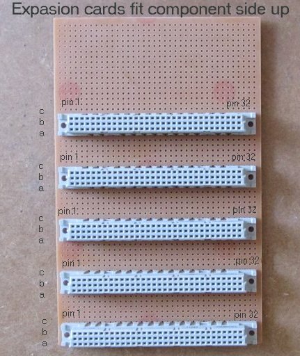
| DIN 41612 connectors come in various forms, type
"C" shown here, has up to 3 rows (a, b, c) of up to 32 pins,
giving a maximum pin count of 96. |
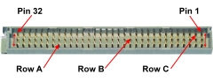 |
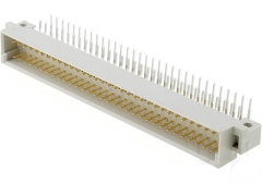
| The connectors that I shall be
using have 2x32 rows of pins in the "a" and "c"
positions, i.e., the middle row is unused.
Male connectors
as shown here will be used on the PCBs
to mate with the female connectors on the backplane.
(Using 96/96 way connectors, screening is
provided on row "b" between each signal track on the
backplane and, via the connector, through onto the
individual cards. If a 64/96 way connector is used,
the 0V screen is still a feature of the backplane) |
 |
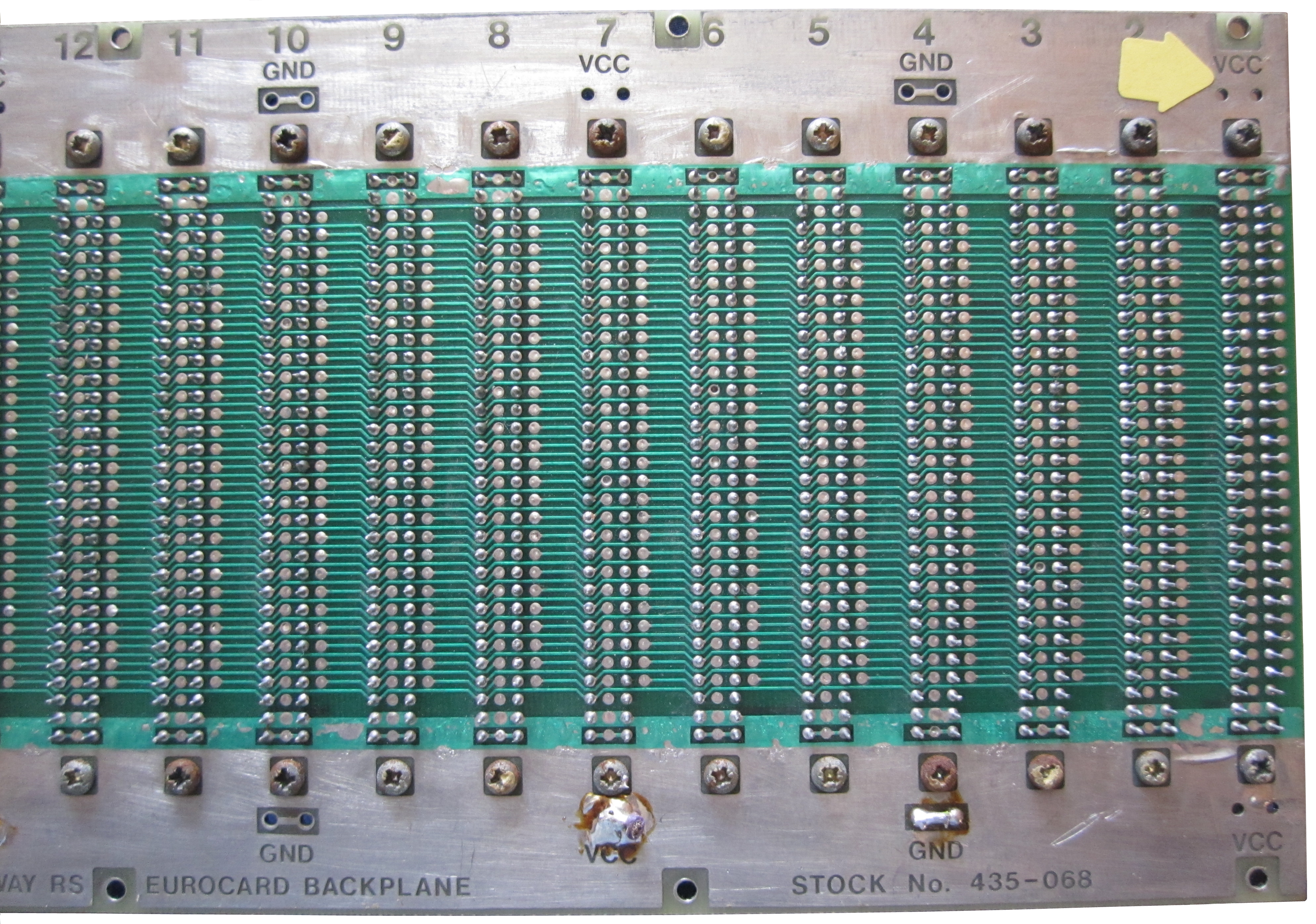
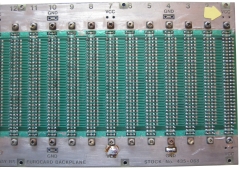
| A close up of the first 12 slots on the solder
side of the backplane.
If you look closely, you may be able to see that
the metal areas on the top and bottom edges provide
separate planes, suitable for dual voltage systems. On this
backplane, the Vcc planes are connected to pin 2
(second pin from the top) and pin 31 (second pin
from the bottom).
The backplane has an RS part number (435-068) and
was manufactured by Vero Technologies as part number
222-2470. |
 |
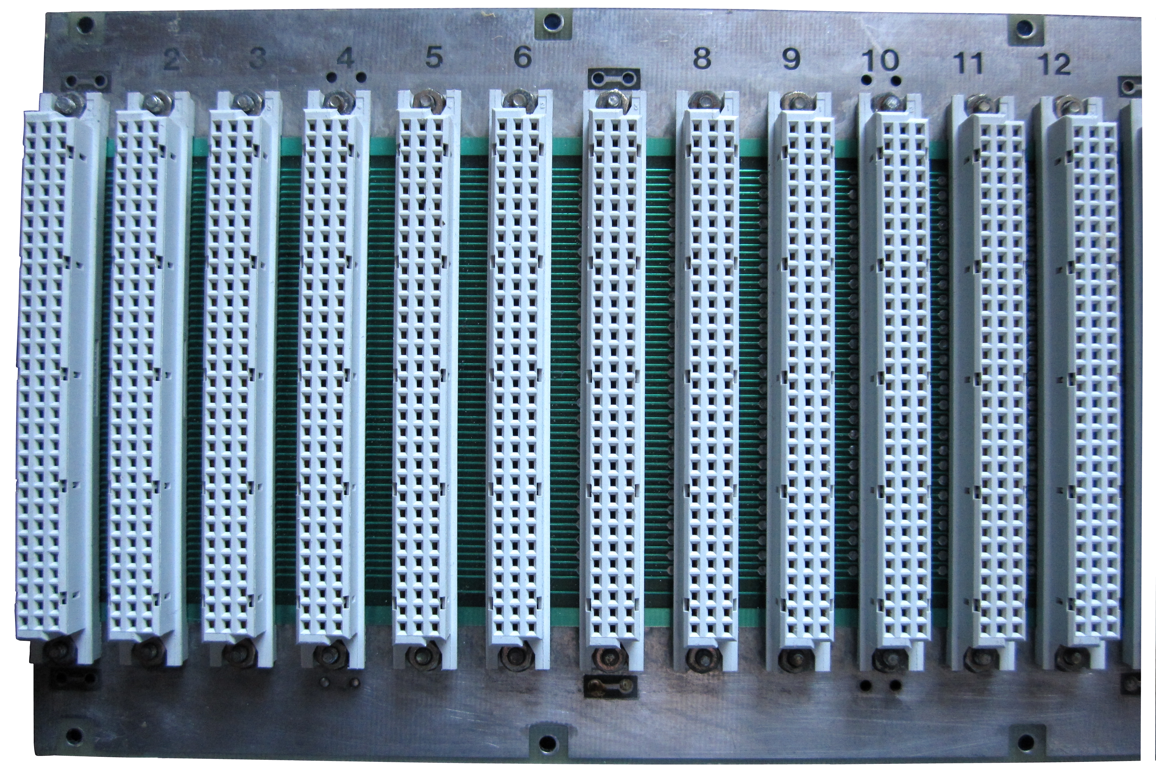
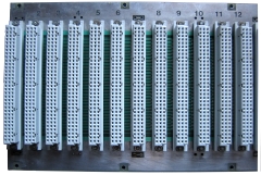
| The front side of the backplane, on this side,
the metal areas on the top and bottom edges provide
separate ground planes, connected to pin 1 (top) and
pin 32 (bottom). (It is possible to cut a track on
the board and assign one of the ground planes to a
third power rail if required.) I don't think that this is
standard and have seen pins 1 and 32 used for power
instead. |
 |
| Of course, a pre-assembled backplane is not
essential. Martin is building his prototype from
scratch - this is his backplane in the process of
being assembled. You can see that Martin's
connectors are spaced further apart than on my
backplane, this will allow the cards to include
taller components and also make soldering of the
connections a bit easier. |
 |
| And the completed version . . . .
The power for Martin's "backplane" will be
supplied by a 40W "wall wart" and the regulators on
the board provide the 12V, 5V and 3.3V regulated
supplies for the PCBs. |
 |
| The solder side of Martin's backplane, showing
the intricate soldering required for the DIN 41612
connectors. Makes me glad that I invested a whole
£5 in a pre-built backplane! |
 |
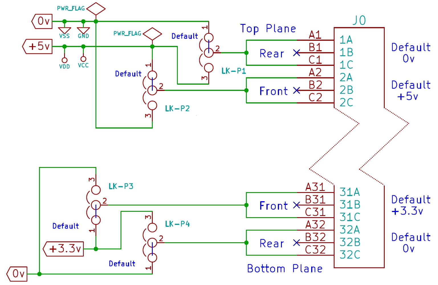
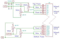
| To cater for different backplane power
distribution, my PCBs will have link options to
allow the Vcc lines to be connected on pins 2 and 31, or 1 and
32 and corresponding selection pins for GND. The
default configuration will have +5v on pin 2 and
grounds on pins 1 and 32. Although not used in an
MTX, the other VCC plane will be used for +3.3v
should it be required for any of the newer logic
chips.
A +12v supply will also be distributed on pin
17c. |
 |
|
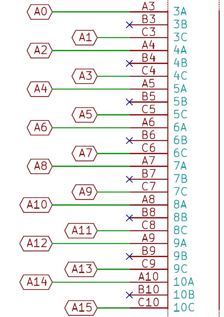
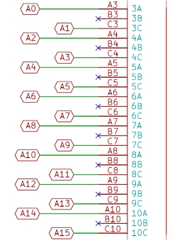
The 16
lines for the Z80 Address Bus are assigned as shown
:
|
Address |
Pin |
Address |
Pin |
|
A0 |
3a |
A8 |
7a |
|
A1 |
3c |
A9 |
7c |
|
A2 |
4a |
A10 |
8a |
|
A3 |
4c |
A11 |
8c |
|
A4 |
5a |
A12 |
9a |
|
A5 |
5c |
A13 |
9c |
|
A6 |
6a |
A14 |
10a |
|
A7 |
6c |
A15 |
10c |
|
 |
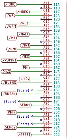
The Z80 Control Bus and system specific control
lines (*) are assigned as shown :
|
Function |
Pin |
Function |
Pin |
|
/IORQ |
11a |
DIAG* |
17a |
|
/MREQ |
11c |
+12v |
17c |
|
/WR |
12a |
/BUSRQ |
18a |
|
/RD |
12c |
(Spare) |
18c |
|
/WAIT |
13a |
/BUSAK |
19a |
|
/HALT |
13c |
(Spare) |
19c |
|
/M1 |
14a |
SER01* |
20a |
|
/INT |
14c |
PHI4* |
20c |
|
/NMI |
15a |
(Spare) |
21a |
|
/IEO |
15c |
(Spare) |
21c |
|
/VDPINT* |
16a |
SER02* |
22a |
|
PHI |
16c |
/RESET |
22c |
* These signals are described on
the CPU board
page
|
 |
|
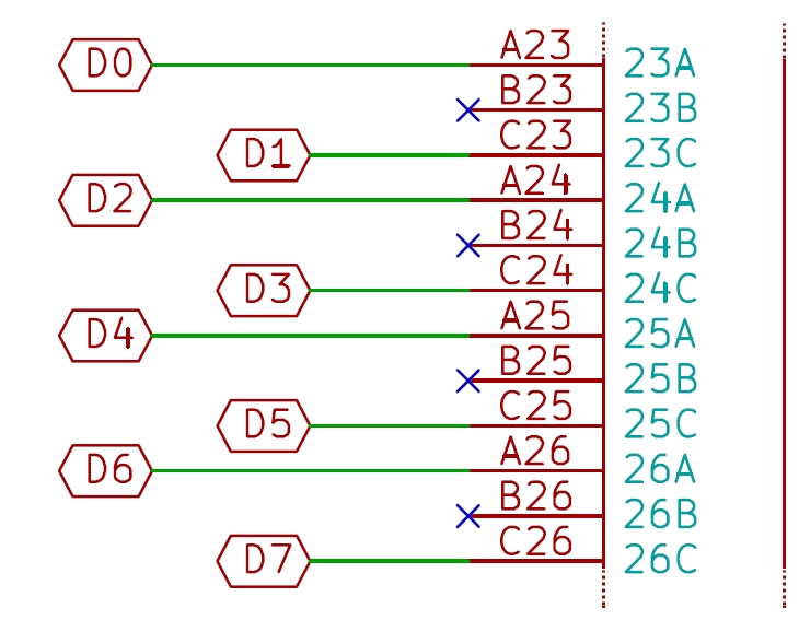
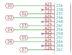
The 8
lines for the Z80 Data Bus are assigned as shown :
|
Address |
Pin |
Address |
Pin |
|
D0 |
23a |
D4 |
25a |
|
D1 |
23c |
D5 |
25c |
|
D2 |
24a |
D6 |
26a |
|
D3 |
24c |
D7 |
26c |
|
 |
|
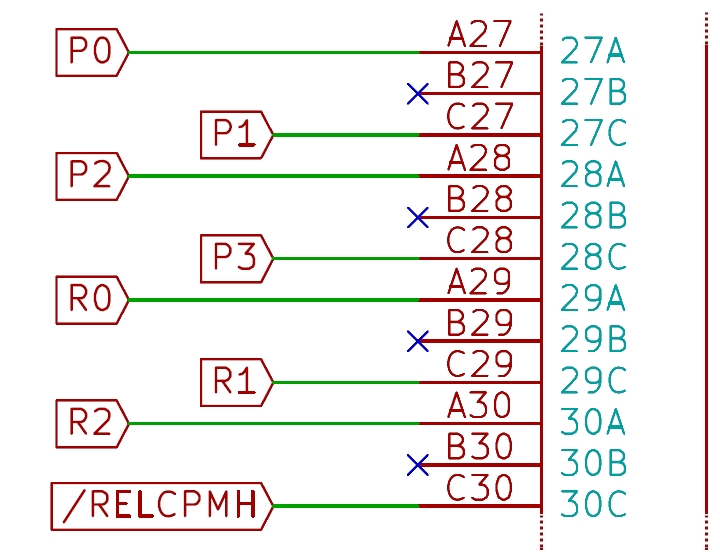
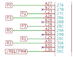
The 8
lines for the MTX Page Port are assigned as shown :
|
Bit |
Pin |
Bit |
Pin |
|
P0 |
27a |
R0 |
29a |
|
P1 |
27c |
R1 |
29c |
|
P2 |
28a |
R2 |
30a |
|
P3 |
28 |
/RELCPMH |
30c |
|
 |
|
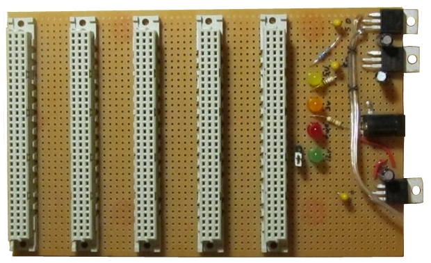
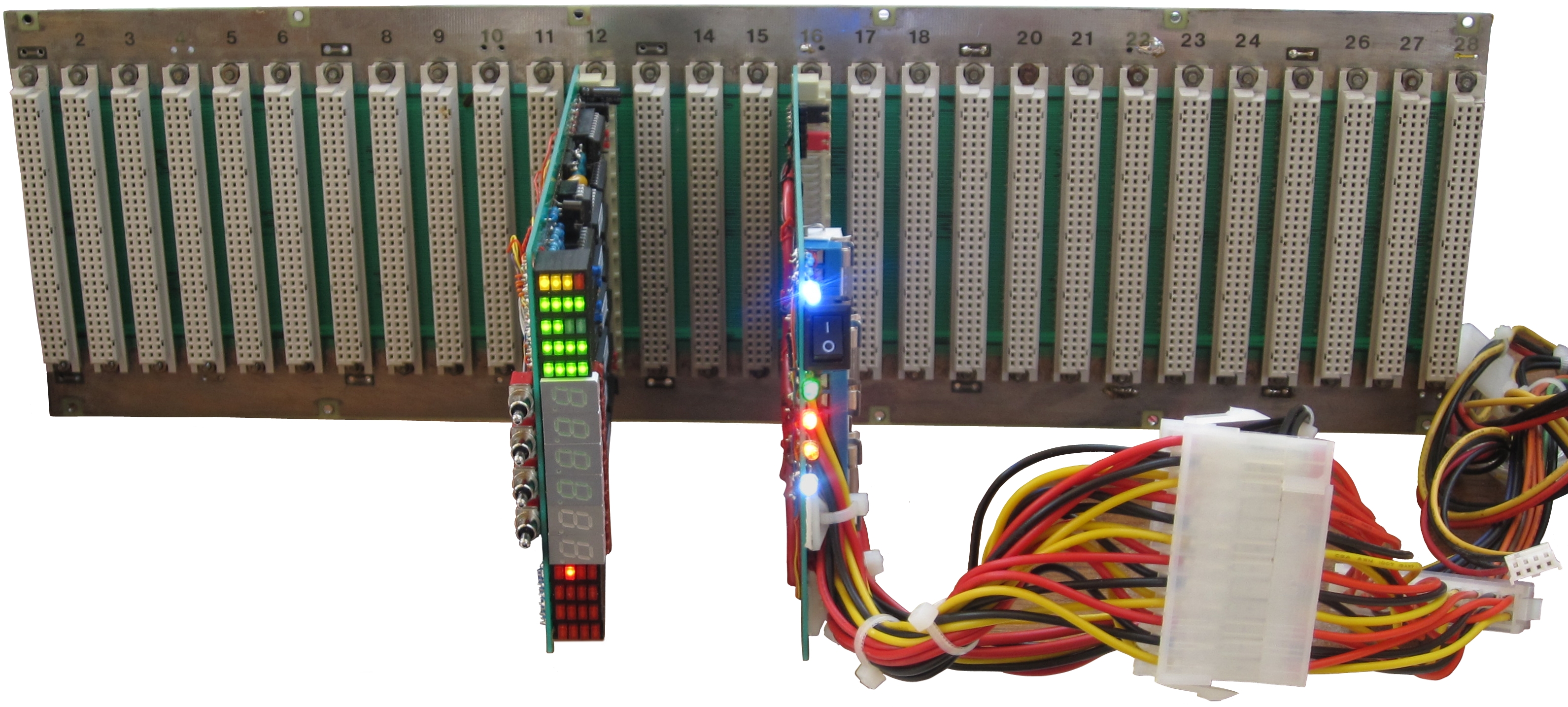
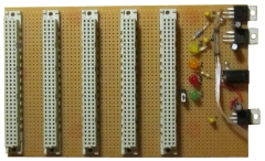
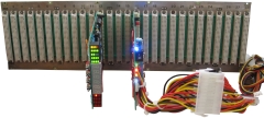
Starting to put the system together . . . Testing
the bus power - the
power board
is on the right, wired to a PC ATX connector for its
power source. The board on the left is the
bus diagnostic
card - showing healthy bus voltages.
|
 |