|
Altera MAX 7128S
I/O
EPM7128SLC84 I/O
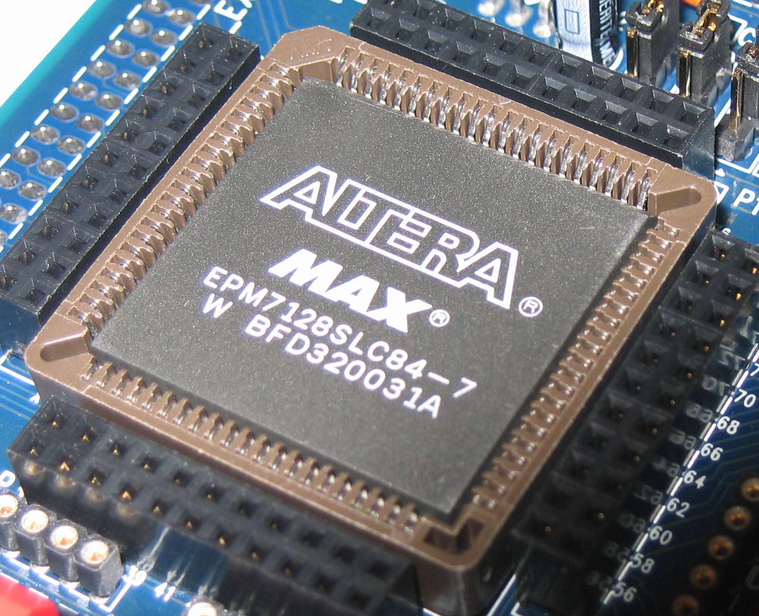
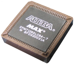
The EPM7128S is available in a number of
packages, but I will only discuss the PLCC option, i.e., the
EPM7128LC84. The photo shows a CPLD inside a chip carrier
which has pins with 0.1" hole pitch, allowing it to be
mounted on prototyping boards. The 84 pin PLCC package has
21 pins on each side, to fit 0.1" hole pitch, the chip
carrier breaks these out into two rows of pins on each side.
 |
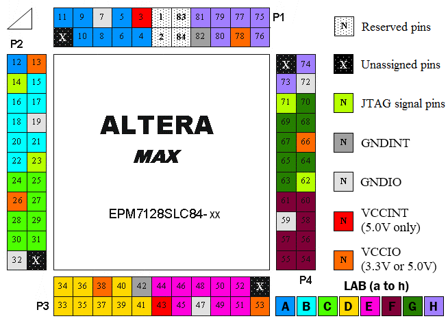
 |
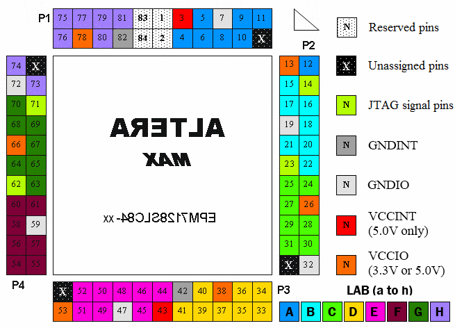
| Chip pin-out |
PLCC Socket pin-out (viewed
from top) |
 |
 |
|
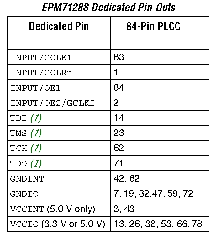
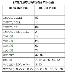
(1) This
pin may be either a JTAG or User I/O pin |
PLCC Socket pin-out
(viewed from bottom) |
|
Reserved
pins |
|
83 |
Global Clock 1 |
|
1 |
Global Clear |
|
84 |
Output Enable 1 |
|
2 |
Output Enable 2 /
Global Clock 2 |
|
JTAG Interface pins |
| 14 |
TDI (Test Data In) |
| 23 |
TMS (Test Mode
Select) |
| 62 |
TCK (Test Clock) |
| 71 |
TDO (Test Data Out) |
|
The PLCC version of the CPLD has a total of 64
User I/O pins, this includes the dedicated input
pins and all I/O pins.
Inspection of the pin-outs shows that each of
the Logic Array Blocks (LABs), has
8 dedicated I/O pins, with one pin on a number
of the LABs, having a dual function, e.g., if a
JTAG interface is used, pins 14, 23, 62 and
71 are used for the JTAG port, otherwise, they
are available as normal I/O pins.
|
|
Power & Ground
There are one set of Vcc pins for internal
operation and input buffers (Vccint), these pins must be
connected to a 5V supply.
Another set of pins are for I/O output drivers
(Vccio), these pins can be connected to either a 5V or 3.3V
supply depending on the output requirements. |
The Altera
Operating
Requirements datasheet advises that 0.2uF
decoupling capacitors should be connected across
each VCC/GND pair.
A 100uF electrolytic capacitor
(subject to not exceeding the VCC rise time :
>1V in 50ms) should be placed next to the power
input terminals to stabilise the power supply. |
|
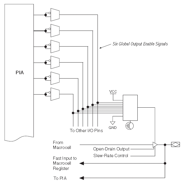
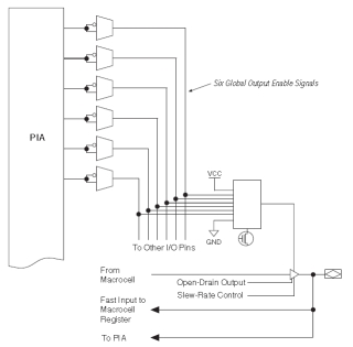
I/O Control Blocks
The I/O control block allows each I/O pin to be
individually configured as input, output or
bidirectional. All I/O pins have a tri-state
buffer that is individually controlled by one of
6 output enable signals or directly connected to
GND or Vcc.
The output enable signals are
driven by the true or compliment of two output
enable signals, a subset of the I/O pins or a
subset of the I/O macrocells.
When the tri-state buffer is
connected to GND, the output is tri-stated and
the I/O pin can be used as a dedicated input,
when the buffer is connected to Vcc, the output
is enabled. |
 |
|
During development of the CPLD
software, the assignment of I/O signals to
individual pins is not required and is best left
until the design is completed. The flexibility
of being able to assign the I/O signals to any
of the I/O pins, regardless of their direction,
means that the physical pin assignments can be
arranged to suit other components and signals
paths on the board.
The "fitter" in Quartus II will
attempt to optimise placement of the logic in
the device to make best use of the available
resources, if the fitter is constrained by user
I/O assignments, it is highly likely that a
non-optimal solution will result. |
The next page discussing signal timing
in the EPM7128S. As Quartus II provides timing
simulation and detailed timing analysis, it is not
really necessary to have a detailed knowledge of the
internal timing and you may prefer to skip straight to
the programming
page.
MAX7128S
Overview <
Previous
Page Goto
Next
Page >
MAX7128S Timing
|