|
Internal Timing Parameters
Within a device, the timing delays
contributed by individual architectural
elements are called internal timing
parameters - these cannot be
measured explicitly. Internal timing
parameters are shown on this page in bold,
italicised, text, e.g., tSEXP
|
|
Speed Grade |
EPM7128S Internal Timing Parameters |
| |
10 |
15 |
Units
xx Max
xx Min |
Parameter - brief
description, see
AN094 for
details |
| tIN |
0.5 |
2.0 |
ns |
Dedicated input delay from
input pad to the PIA |
| tIO |
0.5 |
2.0 |
ns |
I/O input delay from input
pad to PIA |
| tPIA |
1.0 |
2.0 |
ns |
PIA delay, incurred by
routing a signal through the PIA. |
| tSEXP |
5.0 |
8.0 |
ns |
Shared expander array delay |
| tPEXP |
0.8 |
1.0 |
ns |
Parallel expander delay. |
| tGLOB |
1.0 |
1.0 |
ns |
Global control delay. The
delay from a dedicated input pin to any
global control function in a macrocell or
I/O control block. |
| tIOE |
2.0 |
3.0 |
ns |
The delay from an internally
generated signal on the PIA to the output
enable of the tri-state buffer. |
| tLAC |
5.0 |
6.0 |
ns |
Logic array control delay.
The delay for register control functions
such as preset, clear, and output enable. |
| tIC |
5.0 |
6.0 |
ns |
Array clock delay. The delay
through a macrocell’s clock product term to
the register’s clock input. |
| tEN |
5.0 |
6.0 |
ns |
Register enable delay. The
AND array delay from the PIA to the register
enable input. |
| tCLR |
3.0 |
4.0 |
ns |
Register clear time. |
| tPRE |
3.0 |
4.0 |
ns |
Register preset time. |
| tLAD |
5.0 |
6.0 |
ns |
Logic array delay. The time
a logic signal requires to propagate through
a macrocell. |
| tRD |
2.0 |
1.0 |
ns |
Register delay. |
| tSU |
2.0 |
4.0 |
ns |
Register setup time, for
data and enable signals before clock. |
| tH |
5.0 |
4.0 |
ns |
Register hold time, for data
and enable signals after clock. |
| tFSU |
3.0 |
2.0 |
ns |
Fast-input register setup
time. |
| tFH |
0.5 |
1.0 |
ns |
Fast-input register hold
time. |
| tFIN |
1.0 |
2.0 |
ns |
Fast input delay. |
| tCOMB |
2.0 |
1.0 |
ns |
Combinatorial buffer delay. |
| tOD1 |
1.5 |
4.0 |
ns |
Output buffer and pad delay
with the slow slew rate logic option turned
off and V CCIO = V CCINT . |
| tOD2 |
2.0 |
5.0 |
ns |
Output buffer and pad delay
with the slow slew rate logic option turned
off and V CCIO = low voltage. |
| tOD3 |
5.5 |
8.0 |
ns |
Output buffer and pad delay
with the slow slew rate logic option turned
on. |
| tXZ |
5.0 |
6.0 |
ns |
Output buffer disable delay. |
| tZX1 |
5.0 |
6.0 |
ns |
Output buffer enable delay
with the slow slew rate logic option turned
off and V CCIO = V CCINT . |
| tZX2 |
5.5 |
7.0 |
ns |
Output buffer enable delay
with the slow slew rate logic option turned
off and V CCIO = low voltage. |
| tZX3 |
9.0 |
10.0 |
ns |
Output buffer enable delay
with the slow slew rate logic option turned
on. |
| tLPA |
11.0 |
13.0 |
ns |
Low-power adder. The delay
associated with macrocells in low-power
operation. In low-power mode, tLPA
must be added to the logic array delay (tLAD),
the register control delay (tLAC,
tIC,
tACL,
or tEN),
and the shared expander delay (tSEXP)
paths. |
| |
|
External Timing Parameters
External timing parameters
represent the pin-pin timing delays can be
calculated as the sum of the internal
parameters. External timing parameters are
shown on this page in
coloured, bold, italicised, text,
e.g., tPD1
|
|
Speed Grade |
EPM7128S External Timing Parameters |
| |
10 |
15 |
Units
xx Max
xx Min |
Parameter - brief
description, see
AN094 for
details |
|
tPD1 |
10.0 |
15.0 |
ns |
Dedicated input to
non-registered output |
|
tPD2 |
10.0 |
15.0 |
ns |
I/O input to non-registered
output |
|
tPZX |
- |
- |
ns |
Tri-state to active output
delay |
|
tPXZ |
- |
- |
ns |
Active output to tri-state
delay |
|
tCLR |
- |
- |
ns |
Time to clear register delay |
|
tSU |
7.0 |
11.0 |
ns |
Global clock setup time |
|
tH |
0.0 |
0.0 |
ns |
Global clock hold time. |
|
tFSU |
3.0 |
3.0 |
ns |
Fast-input clock setup time |
|
tFH |
0.5 |
0.0 |
ns |
Fast-input clock hold time. |
|
tCO1 |
5.0 |
8.0 |
ns |
Global clock to output delay |
|
tCNT |
10.0 |
13.0 |
ns |
Minimum global clock period |
|
fCNT |
100 |
76.9 |
MHz |
Maximum internal global
clock frequency |
|
tASU |
2.0 |
4.0 |
ns |
Array clock setup time |
|
tAH |
5.0 |
4.0 |
ns |
Array clock hold time. |
|
tAC01 |
10.0 |
15.0 |
ns |
Array clock to output delay |
|
tACH |
4.0 |
6.0 |
ns |
Array clock high time. |
|
tACL |
4.0 |
6.0 |
ns |
Array clock low time. |
|
tCPPW |
4.0 |
6.0 |
ns |
Minimum pulse width for
clear and reset |
|
tODH |
1.0 |
1.0 |
ns |
Output data hold time after
clock |
|
tACNT |
10.0 |
13.0 |
ns |
Minimum array clock period. |
|
fACNT |
100 |
76.9 |
MHz |
Minimum internal array clock
frequency. |
|
fMAX |
125 |
100 |
MHz |
Maximum Clock Frequency |
| |
|
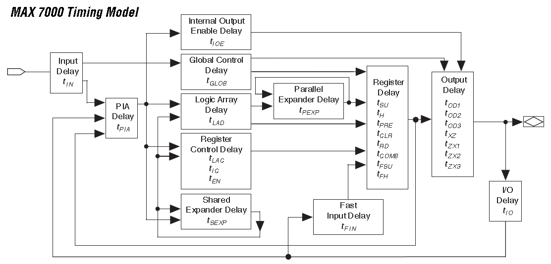
Altera timing models, such as the one for
the MAX7000 series shown at the top of the
page, are a simplified block diagram
that illustrates the propagation delays
through the device. Quartus II can implement
the logic using different paths through the
device, the Report file (.rpt) shows the
equations used to realise the logic and
reveals the actual path through the device.
By tracing the paths through the design and
summing the appropriate timing parameters,
you can calculate the propagation delays
through the device. |