|
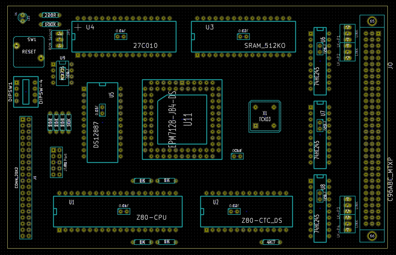
"MTX Plus+" CPU Board V 2.0
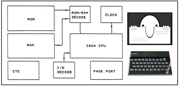
Design Development
Introduction
Before starting construction, the design the CPU board was
more or less finalised but as things progressed, a number of
design changes were made to correct a couple of weaknesses in
the original design. Added to this was some degree of "scope
creep" that led to other modifications.
These "design developments" were originally documented on the
main CPU board page, but the number and magnitude of the changes
probably justifies their description on a separate page - ergo -
this page!
CTC Clock Frequency
(Design error)
In my original design for the CPU board, the Z80 CTC was
intended to run off the fixed 4MHz clock, rather than running at
the same speed as the CPU. When Martin and I were trying to work
out what the various issues with the CPU board might have been,
I wondered whether this might have had a bearing on the problems
that we were seeing.
I did some tests running the CTC at the same speed as the
CPU, whilst testing showed that this did not actually appear to
make a difference, and the Zilog documentation does not
explicitly say that this is required, further reading of the CTC
data sheet does suggest that the two are intended to run in
sync. Therefore, the design was modified to run the CTC from
the PHI, rather than the PHI4, clock.
Whilst initial testing has not identified any problems with
running the CTC at 16MHz, this is well in excess of the
specification of the 8MHz CTCs that we have available.
However, given the good results Martin has had over-clocking a
genuine Zilog 10MHz CPU, we are hopeful that the CTC can be
over-clocked to the same degree. Failing that, the fastest
available DIP packaged Zilog CTC is 10MHz, so a slightly faster
option is available should the need arise.
Address Buffers
(Design optimisation)
As described in
this entry on the
notes
page, the Address Buffers were installed such that they only
buffered the address lines going off the CPU board onto the
backplane. The preferred location is to have the input side of
the buffers connected directly to the Z80 address pins and have
everything else connected to the output side of the buffers.
As well as being "best practice", an additional feature that
is being planned (more details if/when it has been proven) would
require that the buffers were close-coupled to the CPU with
everything else on the output side. Although the work required
to change the buffer wiring was not insignificant, I have now
changed the logical position of the address buffers as
described, the revised buffer position is shown in board
revisions from version 2.09.
When the Z80 CPU is in control of the Address buffers, i.e.,
it has not passed over control of the buses in response to
BUSRQ
being asserted by another device, such as a DMA controller, the
only meaningful direction for data through the address buffers
is from the CPU out - A to B in my schematic, when the CPU puts
a target memory or I/O address on the bus. The '245s used in my
design are overkill as having the CPU read addresses being used
by the external device is pointless. Something like a '244 is a
more logical choice with the outputs either being controlled by
the CPU or just tri-stated when not. Should MTXPlus+ ever make
it to the stage of getting a PCB manufactured, I will update the
design to use '244 buffers for the address lines.
Address Buffers have been removed from the final version of
the board - see comment under Control Bus
Buffering
Data Buffer
(Design error & Design optimisation)
During testing of the CPU boards, neither board would not
operate unless the 74HC245 data buffer that I had positioned
between the on-board data bus and the backplane was bypassed,
indicating that the problem was in the design, rather than
construction. Being unable to work out the problem and not
wanting to try rewiring the buffer without really
understanding what the problem was, I resorted to calling for
help from Tony Brewer, an ex-Memotech programmer & designer and
Z80 guru. Tony immediately pointed out the error of my ways -
more details in
this
entry on my
Notes page.
In addition to modifying the incorrect logic for the data
buffer direction control, I have also changed the logical
position of the data buffer to connect it directly to the CPU
data bus pins, with everything else on the "B" side of the
buffer. Both sides of the buffer now have weak pull-up resistors
(10k) fitted to stop the bus from floating when disconnected.
The Data Buffer hasbeen removed from the final version of the
board - see comment under Control Bus
Buffering
Memory Address Lines
(Design optimisation)
To cater for memory addresses >65535 (216),
additional address lines beyond the Z80's A0
to A15 are required. In MTXPlus+,
decoding of these address lines is being done in either a CPLD
or two PLDs. Initially, although using different technology, the
logic for these address lines was going to be functionally
equivalent in the CPLD and PLD solutions and the boards wired consistently.
The limited number of product terms available in the PLDs
being used means that, even though RAM and ROM are never
accessed simultaneously, separate address lines are required for
them, labelled on the schematic as OA14
to OA18 for the RAM and RA13
to RA15 for the ROM
The CPLD has far greater capacity for combinatorial logic
than the GALs being used, but, although the I/O pin count is
also far greater than the GAL, it is easy to run out of physical
connections before the logic capacity of the CPLD becomes a
limitation. Since I wanted to use some of the spare capacity in
the CPLD (for non-core MTXPlus+ functionality) there were good
arguments for following up on a suggestion by Tony Brewer to
multiplex the address lines to reduce the "wasted" CPLD I/O,
freeing the CPLD RA13, RA14 and RA15 pins for other purposes.
The schematic and CPLD ROM/RAM decode logic has now been
updated to reflect this design - the PLD solution is unchanged
by this modification.
VDP Update Speed
(Enhancement)
Given my limited, OK then - non-existent, Z80 programming
skills, one of the design goals was to make MTXPlus+
fully backward compatible with the original MTX computer so that
I could just drop in a copy of the Memotech ROMs and have a
working system while I tried to figure out how to write a CP/M
BIOS for the machine to take full advantage of its updated
hardware. It was recognised that this would mean that MTXPlus+
would likely only run as an MTX clone at 4MHz, as many of the
ROM routines for such things as video, sound, time, cursor flash
etc. would have been optimised for 4MHz operation.
When designing the video board, I was mainly focused on the
hardware and spent little time going over the technical
documentation (schoolboy error). I was aware that one of the
enhancements in the V9958 was the inclusion of a WAIT function
that was designed to allow the VDP to throttle VRAM access at
higher CPU speeds by asserting the Z80
WAIT line to pause the CPU as required. However,
although I had included this feature in the board design, I had
not realised that the VDP WAIT function is disabled by default
(see below).
Even without the MTX ROM, when testing the video board at
16MHz, a large number of CPU delays (using the Z80
NOP
opcode) were
necessary to comply with the speed constraints of the VDP and
VRAMs. At that stage, it was envisaged that the eventual MTXPlus+
operating system and the original MTX ROMs would need to be
patched to insert wait states for writes to the VDP.
However, there proved to be a better way, that is, by having
the required delays being inserted automatically. Tony Brewer
spotted that I had missed the fact that the default state for
the V9958 WAIT function is disabled, when this was enabled (by
setting bit 2 of Control Register #25), we found that with CPU
clock rates up to 8MHz, the VDP's WAIT function was able to
throttle VDP VRAM access as required. At higher CPU speeds
though, some simple additional logic was required to be
implemented in a PLD. When I say "simple", the concept is
simple, but the idea and implementation is the result of many
years experience of Z80 system design and programming by Tony.
Tony designed logic that will execute in an additional GAL22V10 that can
be fitted to the video board. The logic will utilise
the I/O address decoding already done in the existing video
board GAL to
detect VDP accesses and then, using the 8MHz clock signal, will
determine the required length of time to pause the CPU to allow
the VDP access to complete. The required delays will be enforced
in the same was as the VDP does for lower speeds, i.e., by asserting the Z80
WAIT line to pause the CPU as required.
Further details of the Video speed control logic can be found
on the Video firmware
page
Control Bus Buffering
(Evaluated and subsequently removed)
My original design did not have buffers on the Z80 control
bus lines, Steve Ciarcia's "Build Your Own Z80 Computer" was
based on using an NMOS Z80 CPU and standard 74 series logic and
advised that the Z80 could sink a "maximum 1.8mA or 1 TTL load
on each pin". Using 74LS series logic, the fan-out from each pin
of the NMOS Z80 could have been increased to 9, this would have
been ample for Ciarcia's ZAP (Z80 Applications Processor)
computer, but to illustrate how larger systems could be
constructed, buffers were added to the address, data and control
buses. For the control bus, the buffer for each line was just a
pair of back-to-back 7404 inverters to provide both inverted and
non-inverted buffered control lines.
The original MTX computer did not have buffers installed on
the main computer board's address or control buses and only
buffered the data bus for the output ports.
Based on the above, as well as some "helpful", if misleading
advice, I chose to only install buffers for the address and data
buses as they left the CPU board, rather than the correct
location at the output pins of the Z80. I also decided that
buffering the control lines would not be necessary, particularly
using CMOS logic where the fan-out capability is much larger and
certainly beyond a level that would be an issue in my design for
MTXPlus+.
However, even though the control bus signals have not been an
issue during testing of the CPU board, to follow "best practice"
and mitigate any risk in not having them should I eventually get
a PCB manufactured, I decided that I should really add buffers
to the control bus too.
Initially, my intention was to use an octal buffer, probably
another 74HC245, but due to some "scope creep", I also had a
requirement for a small amount of additional logic that could
not be done in the CPLD due to a lack of resources. To satisfy
both requirements, control bus buffering
logic was designed for implementation in an additional GAL22V10 installed on the CPU
board.
As it turned out, the additional delays introduced by adding
the buffer was detrimental to the overall performance and the
system proved to be capable of running faster without it. Since
the system mainly uses CMOS components which supports more
fan-out connections (~50) than TTL (~10), control bus buffering
has not been implemented.
For similar reasons, the buffers in the Address and Data
lines have also been removed from the final PCB design.
CPU Speed Selection
The clock signals on the CPU board are all derived from a
single 32MHz oscillator, on my board, all of the sub-clocks are
generated inside the CPLD, on Martin's board, they are generated
using two 74HC193 4-bit counter chips. The base design called
for a 16MHz CPU clock (PHI), 8MHz (PHI8), 4MHz (PHI4) and
two clocks for the serial ports (SER01 & SER02), these are
all allocated space on the bus. With all of the
logic required for the base scope of the project configured,
there was ample space for me to generate an number of additional
clocks that could be used during the testing phase, including
2MHz, 1MHz, 1KHz, 8Hz, 2Hz and 1Hz. Selection of 8 system speeds
could be done using 3 bit-switches, PS0, PS1 and PS2.
In light of the "scope creep" noted above, and to free up
resources for the "Mystery Upgrade", I
decided to forgo some of the slower test clocks and reuse some
of the CPLD logic and I/O capacity and rationalise on 16, 8 and
4 MHz clocks, as well as a single, configurable "slow" clock. A
reduction in the number of slow clocks is, to a large extent,
mitigated by the ability to have the processor single step using
the Diagnostic board.
As the design developed, Tony Brewer got more deeply involved
in the logic design for the CPU CPLD and was able to devise a
method that allowed the CPU clock frequency to be switched in
real time using I/O Port 255
Further details of the CPU clock logic can be found on the
CPU Clock firmware
page
CPLD Upgrade
The "Mystery Upgrade" currently in development, requires a
few more resources than were free in the original Altera
EPM7128S CPLD. The EPM7160S is a slightly more powerful device
with 160 macro-cells, the PLCC version is virtually
pin-compatible with the '7128, but 4 of the I/O pins are
unavailable, the reduced I/O count of the 7160 is the main
reason that the additional GAL is necessary.
Mystery Upgrade
The "Mystery" Revealed
- Courtesy of Tony Brewer - Turning MTXPlus+ into a
Sinclair ZX
Spectrum, introducing,
Speculator+
Further details of the Speculator+ logic can be found on the
Speculator+
firmware page
|