|
"MTX Plus+"
Firmware
 |
|
|
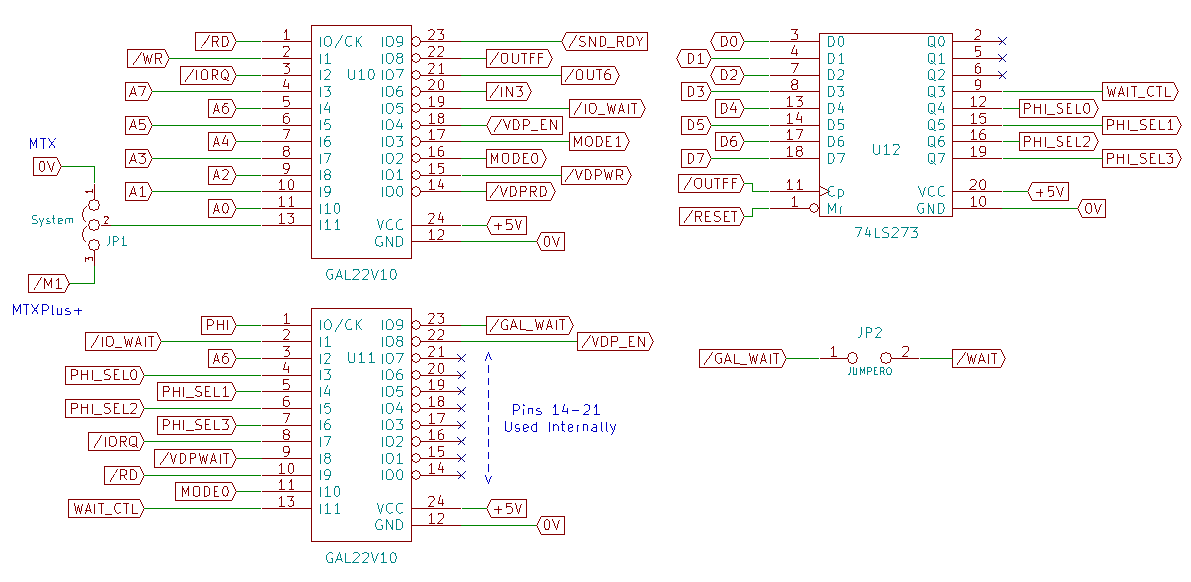
VS1 GAL |
VS2 GAL |
Video Board
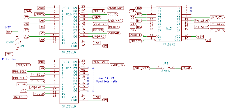
CPU Wait State Generation for VDP and PIA
CPU
clock speeds above about 6MHz exceed the specifications for the
VDP, PSG and the PIA used to drive the CF interface. To allow
these slower parts to be used at the higher clock frequencies,
one of the GALs on the video board inserts WAIT states during
I/O operations on these devices.
The
Technical Manual for the Yamaha V9958 indicates that the minimum
delay between VDP accesses is just over 2 µs.
GAL
"VS1" (U10) on the video board is a GAL22V10 that does I/O port
decode and generates the "normal" VDP and PSG control signals
(MODE 0, MODE 1, VDPWR,
VDPRD,
IN3 &
OUT6). If MTXPlus+
only operated at clock frequencies lower than the maximum rated
speeds of the VDP and PSG, then no additional throttling
functionality would be required.
GAL
"VS2" (U11) was added to provide a mechanism for delaying
consecutive VDP I/O operations to ensure that the minimum time
between them did not exceed the capabilities of the VDP. The
IO_WAIT
output from VS1 is active when a I/O port operation is being
performed on the VDP (or PSG).
Initially, VS2 used 4 bit switches to allow the user
to manually specify the number of Z80 "T" states to insert
between consecutive VDP I/O operations. Although this worked
satisfactorily, having a fixed delay time meant that if the bit
switches were set to allow operation at the highest clock speed,
then unnecessary delays were being inserted at lower speeds.
The
addition of functionality to allow the CPU
clock frequency to be
set in software means that the length of the delay between
VDP I/O operations can be set to the optimum value for each PHI
rate automatically. When the system clock rate is changed by
writing to the system control port (FFh), VS1
generates the OUT_FF signal
that is used to latch the control signals being sent to port FF,
i.e., to store the state of the commanded system speed.
A
74xx273 octal flip-flop on the video board is used to store the
values of bits D7 to D0 when the system control port (FFh)
is updated when the system speed is set through software or by
Speculator+. Bits D7 to D4 indicate which of the 16
available clocks have been selected, bit D3 is updated by
Speculator+ to disable wait state generation during the NMI
interval when Speculator+ is running. Bits D2 to D0 are
currently unused by logic on the video board but are stored in
the flip-flop for possible future use.
Bits D7
to D4 in the system control word have been used to replace the
bit switch inputs to VS2, meaning that the required delay
between VDP I/O operations is tuned to the current system clock
speed.
GAL VS2
contains a 7 bit counter (6 bits used) which is seeded with the
values shown in the table below for each clock rate, for
example, when clock rate 11 (10.67 MHz) is selected, the counter
is seeded with the value 31d. Consecutive VDP
accesses are delayed until the counter has counted down to zero
by asserting the CPU WAIT
signal. The rightmost column shows the actual delay in µs
inserted for each clock rate.
|
|
|
VS2 GAL Counter Value |
|
|
Clock |
D7 |
D6 |
D5 |
D4 |
Q6 |
Q5 |
Q4 |
Q3 |
Q2 |
Q1 |
Q0 |
Dec |
µs |
| 0 |
0 |
0 |
0 |
0 |
- |
0 |
0 |
1 |
1 |
0 |
0 |
12 |
3.3* |
| 1 |
0 |
0 |
0 |
1 |
- |
0 |
0 |
1 |
1 |
0 |
1 |
13 |
3.1 |
| 2 |
0 |
0 |
1 |
0 |
- |
0 |
0 |
1 |
1 |
1 |
0 |
14 |
3.0 |
| 3 |
0 |
0 |
1 |
1 |
- |
0 |
0 |
1 |
1 |
1 |
1 |
15 |
3.0 |
| 4 |
0 |
1 |
0 |
0 |
- |
0 |
1 |
0 |
0 |
0 |
1 |
17 |
3.1 |
| 5 |
0 |
1 |
0 |
1 |
- |
0 |
1 |
0 |
0 |
1 |
1 |
19 |
3.1 |
| 6 |
0 |
1 |
1 |
0 |
- |
0 |
1 |
0 |
1 |
0 |
1 |
21 |
3.1 |
| 7 |
0 |
1 |
1 |
1 |
- |
0 |
1 |
0 |
1 |
1 |
1 |
23 |
3.0 |
| 8 |
1 |
0 |
0 |
0 |
- |
0 |
1 |
1 |
0 |
0 |
1 |
25 |
3.0 |
| 9 |
1 |
0 |
0 |
1 |
- |
0 |
1 |
1 |
0 |
1 |
1 |
27 |
3.1 |
| 10 |
1 |
0 |
1 |
0 |
- |
0 |
1 |
1 |
1 |
0 |
1 |
29 |
3.0 |
| 11 |
1 |
0 |
1 |
1 |
- |
0 |
1 |
1 |
1 |
1 |
1 |
31 |
3.0 |
| 12 |
1 |
1 |
0 |
0 |
- |
1 |
0 |
0 |
0 |
1 |
1 |
35 |
3.1 |
| 13 |
1 |
1 |
0 |
1 |
- |
1 |
0 |
0 |
1 |
1 |
1 |
39 |
3.1 |
| 14 |
1 |
1 |
1 |
0 |
- |
1 |
0 |
1 |
0 |
1 |
1 |
43 |
3.1 |
| 15 |
1 |
1 |
1 |
1 |
- |
1 |
0 |
1 |
1 |
1 |
1 |
47 |
3.0 |
| *
Irrelevant as waits are disabled when D7..D4 =
0000 |
|