This somewhat lengthy page is intended
to give an insight into the effort that Martin puts in when
designing add-ons for the MTX, this time, it was MFX. The page evolved as Martin kept
me posted on his progress, it does not capture the detail of the
many hours that Martin explored and resolved numerous minor
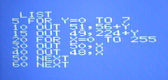
issues that emerged as the design progressed. It does hopefully
give an indication of the design process and major milestones
along the way. I hope that you find it interesting - I do !
If you want to read about my turning the
prototype into a "product", see the MFX
Engineering page
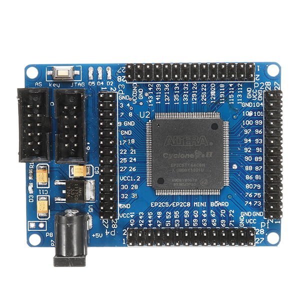
When
looking for a suitable FPGA development board that might
be incorporated into a new MTX expansion card design, I did a little "Googling" and came across
this minimum system development board based on the
Altera Cyclone II FPGA.
The
Land Boards wiki has some details about the board. |
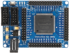 |
The
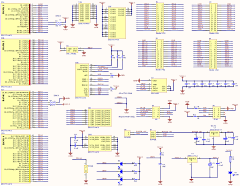
Art of circuits website has a copy of the schematic.
Some of the FPGA's I/O are assigned to on board
components that you might need on a development board, including user LEDs,
a power LED and a push
button. In addition, some pins are connected to Vcc or
Gnd which are not required if the board uses an EP2C5
and could potentially be freed up if required.
(This information only came to light as the design
progressed.) |
 |
When I suggested it to Martin, it
turned out that he already had one!
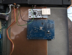
This board has been
around for quite a while now and
Grant Searle had used the
board a few years ago as the basis of his
Multicomp project - creating a number of different micros
using the same FPGA development board, and Martin had
implemented it himself as shown here.
Other than a few passives and I/O
connectors, the only additional component is a RAM chip. |
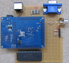 |
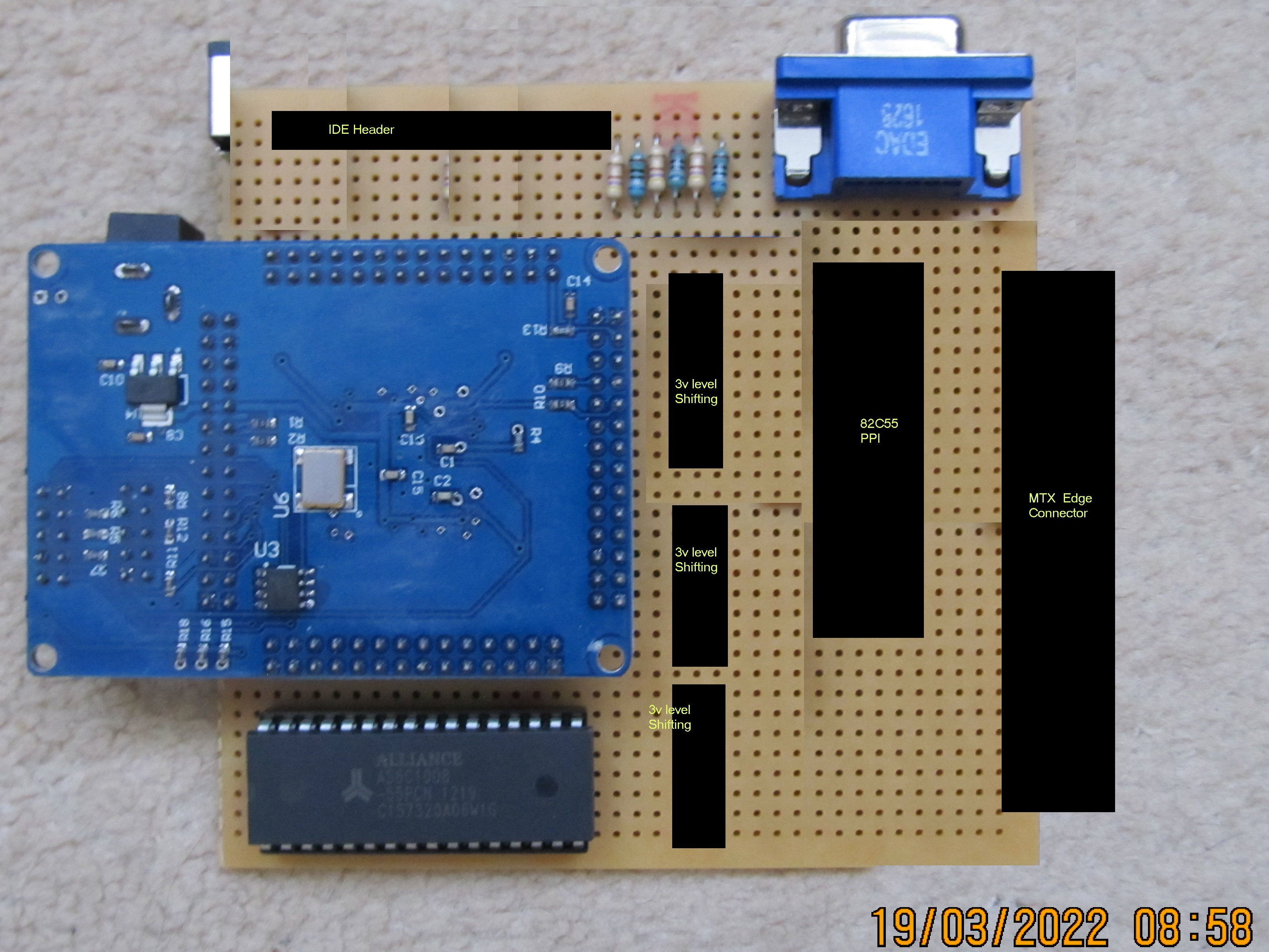
At this
point, we were still thinking about a CFX replacement
and Martin did a mock up sketch of how an external MTX
add-on board might look. Note the presence of the 82C55
PPI intended to provide the CF interface.
After
further discussion we agreed that the CF card would be
better replaced with an SD card interface - particularly
when the majority of the required FPGA code had already
been developed by Andy for REMEMOTECH ! |
 |
Our previous MTX
expansion boards such as CFX
and MAGROM had all
been designed to be smaller than 100mm x 100mm to meet a
price point of the low cost PCB manufacturers that I had
used in the past. However, given that I really wanted to
design something that would fit inside the MTX case
(which has reduced depth at the front, restricting the
area available for mounting higher profile devices, such
as the FPGA board), we agreed that the footprint would
be larger for MFX than for our previous boards.
We also wanted to include the network interface that
Martin had previously designed (NFX)
and the desire to add an SD card slot on a daughter
board, rather than as an SMT component, all meant the
the board was going to be quite a bit larger than
those of our previous projects.
With a prospective list of
components, including :
VGA output connector
Video
RAM
SD card interface header
WIZ810 headers
System RAM
CP/M Boot ROM
Decode logic for WIZ810
& MTX side RAM
Level shifting for FPGA to MTX
signals.
The board was definitely going to be
bigger than 100mm square, but if it could be kept to the
size of a
Eurocard PCB, it would fit the PCB guide slots inside the
MTX case perfectly. |
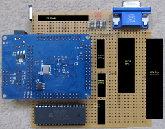
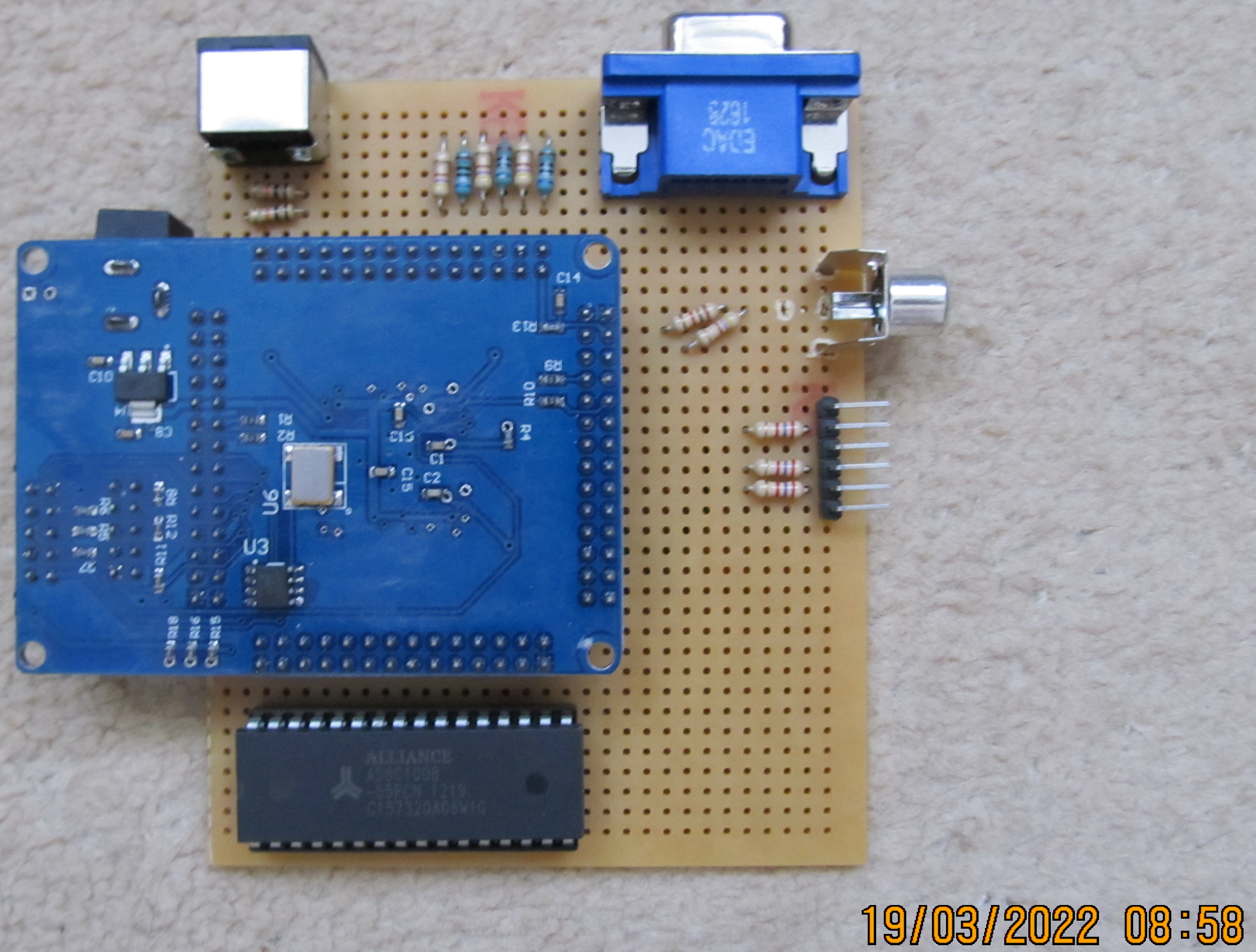
Martin did
a test fit of the WIZnet and FPGA development boards
mounted on a Eurocard sized piece of prototype board
and confirmed that there should be enough space to mount all
of the components inside the case. (The phono connector
above the WIZnet module is not present on a standard MTX
- it's Martin's way of accessing the MTX video output.)
It can be seen
that the mock up is the same depth as the MTX computer
board and so fits nicely in the MTX case's PCB guides. |
 |
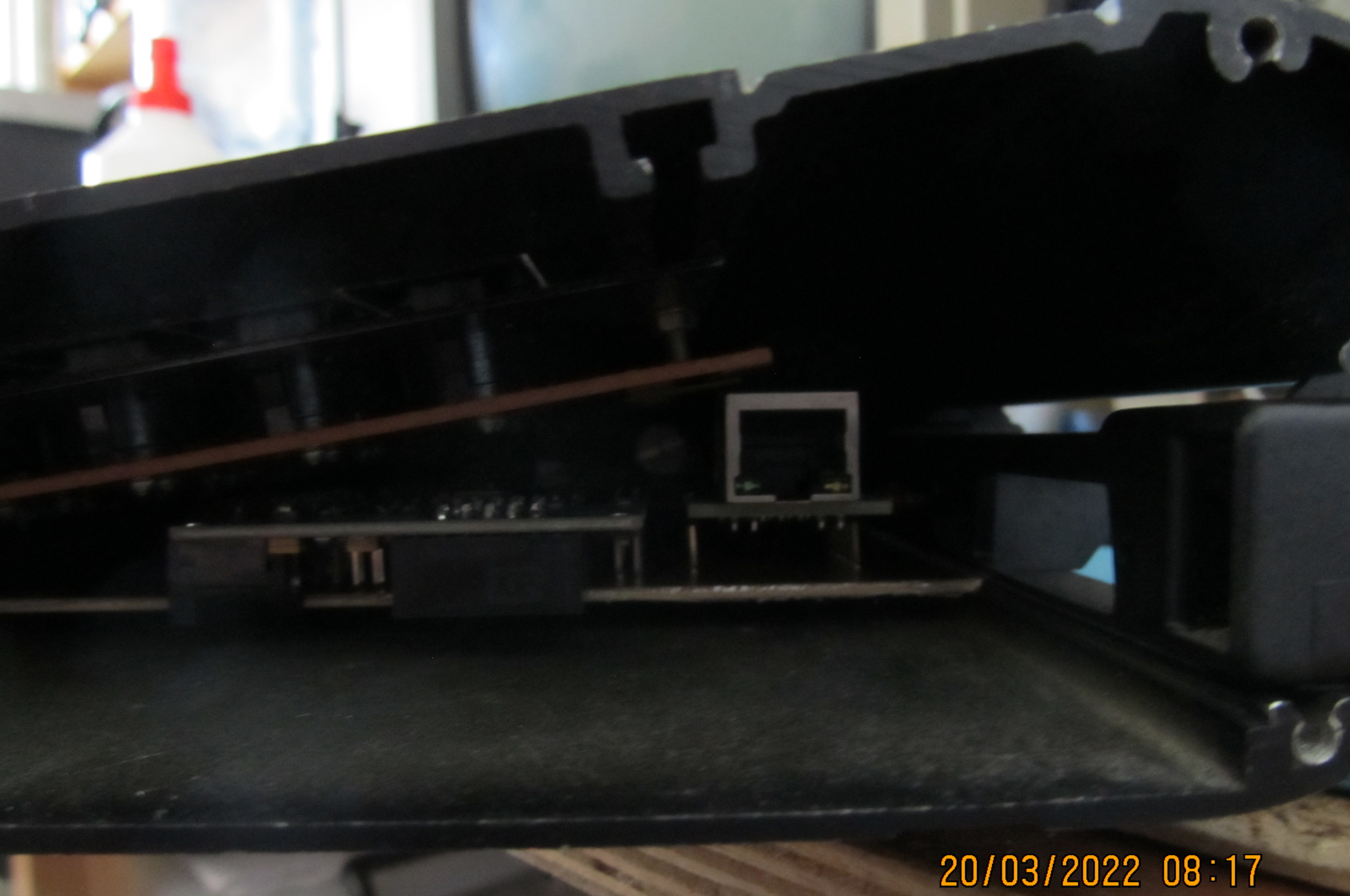
Space is
tight, but there is adequate clearance below the
keyboard PCB.
For this to work, the MFX PCB would
need to be at the same level as the MTX computer board,
i.e., the connector between the two boards would need to
be straight, like the original Memotech ones, rather
than the angled PCB connectors used for our previous
boards. Such connectors are available, but have long
lead times and are more expensive. |
 |
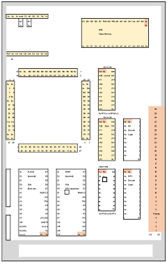
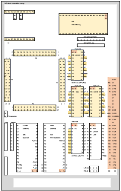
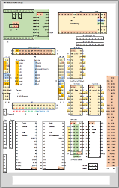
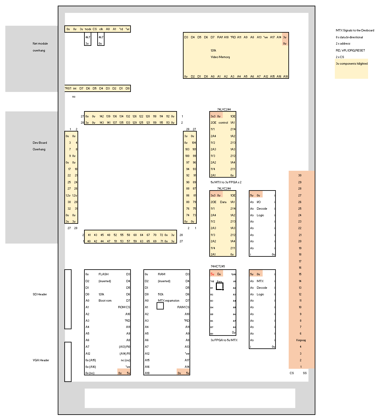
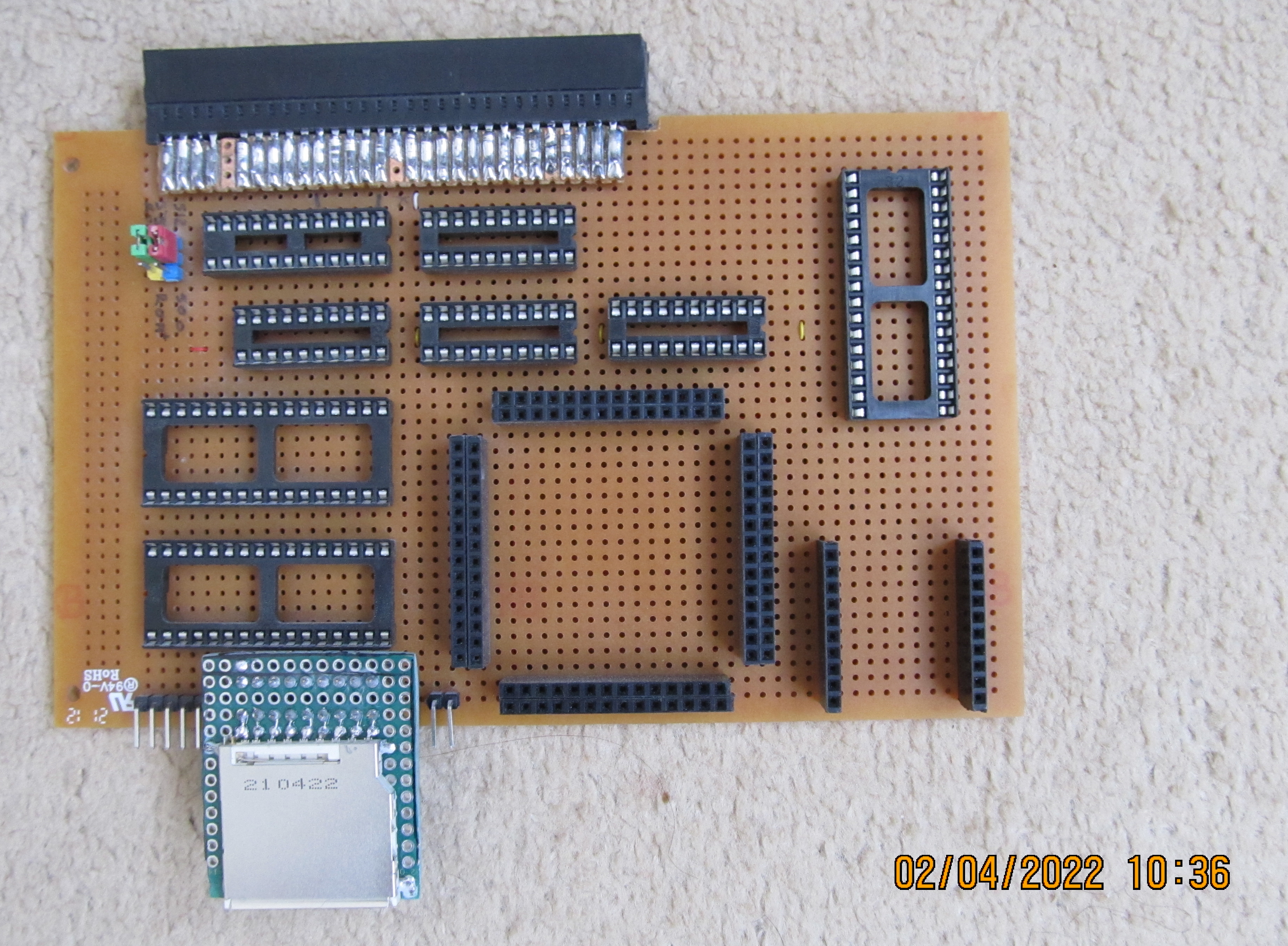
Martin's
first version of a possible layout for the MFX board.
As usual, the layout is intended to guide Martin
during the wiring of his prototype board and is
therefore viewing the board from below, the board would
be "flipped" to mount inside the MTX, so the orange
strip at the right side would actually be located
adjacent to the internal J0 connector on the MTX
computer board.
Martin's prototype uses a
Eurocard prototype board intended to have a
DIN
41612 connector at one end. Although this will not
be used by MFX, it is likely that a second MTX connector
could be mounted in this area to allow the MFX board to
be connected externally if required.
This
provisional layout includes for sockets for the pin
headers of the FPGA and WIZnet modules and for header
pins for the SD card and VGA connectors.
Sockets
are provided for 128kB Video RAM, 128kB boot ROM and
512kB RAM chips as well as GALs for RAM and I/O decode
logic and level shifters for the connections between the
MTX (5v) and FPGA (3v). |
 |
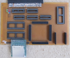
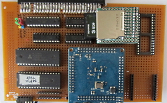
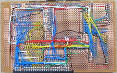
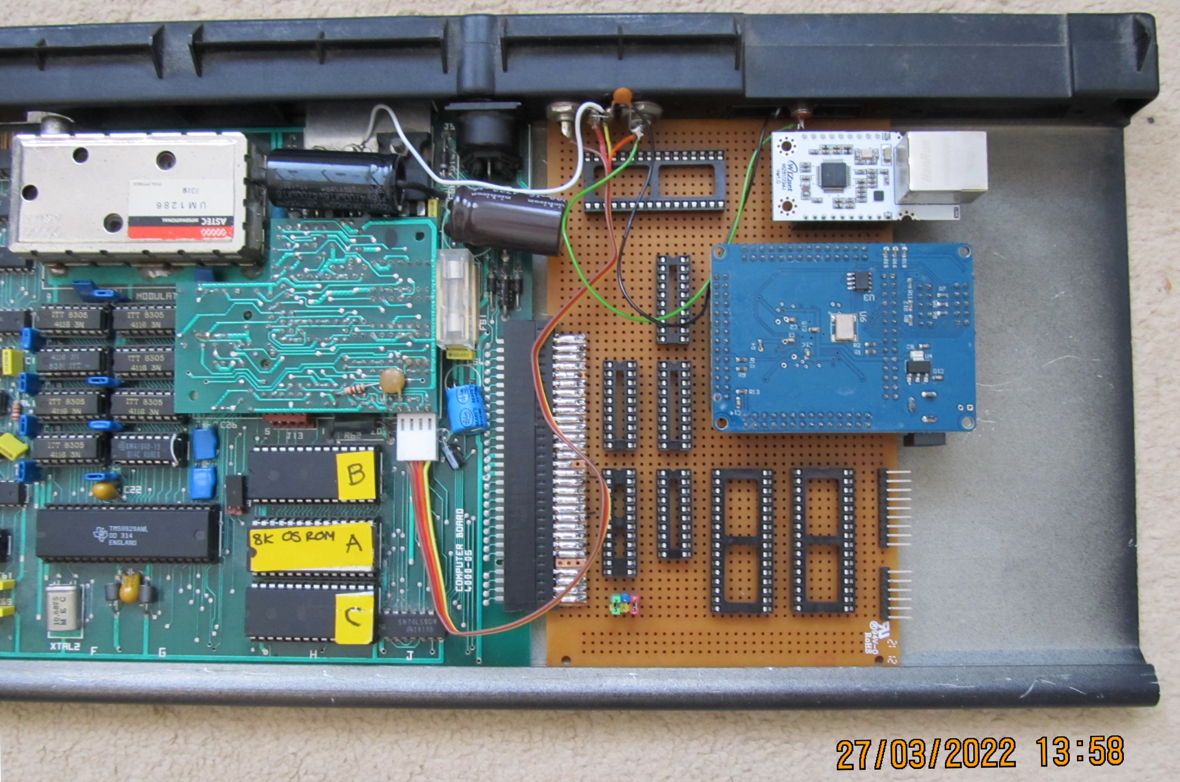
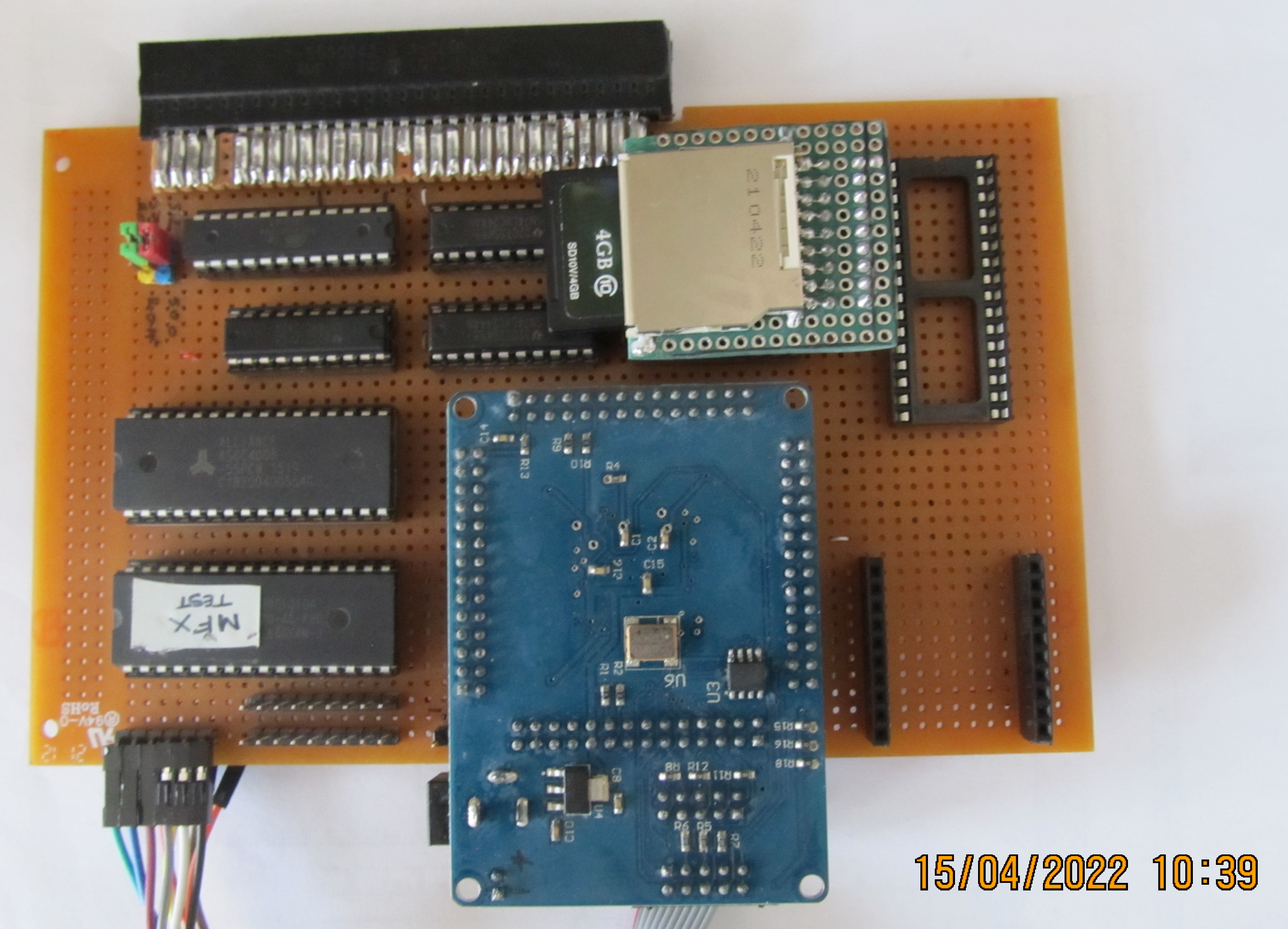
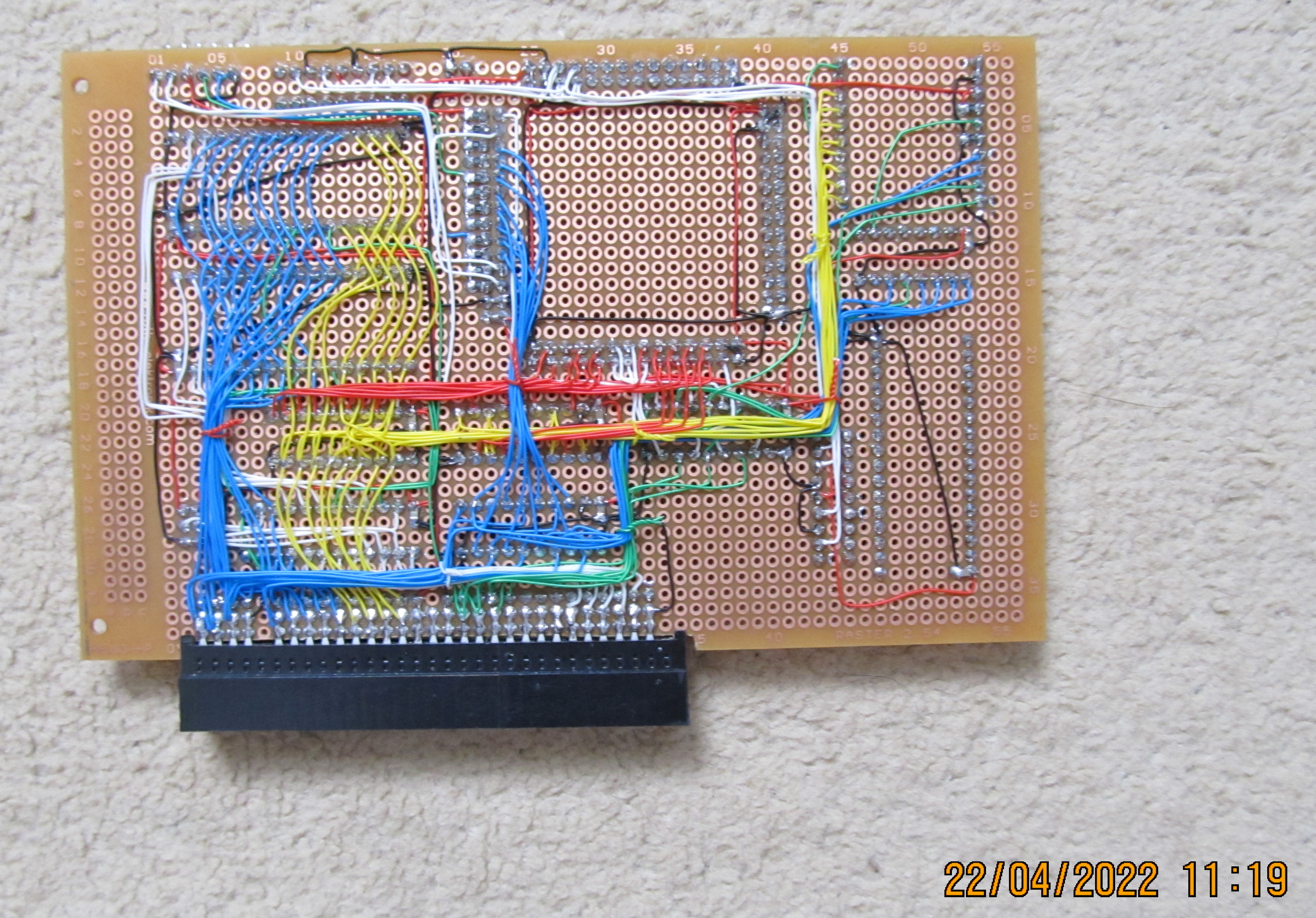
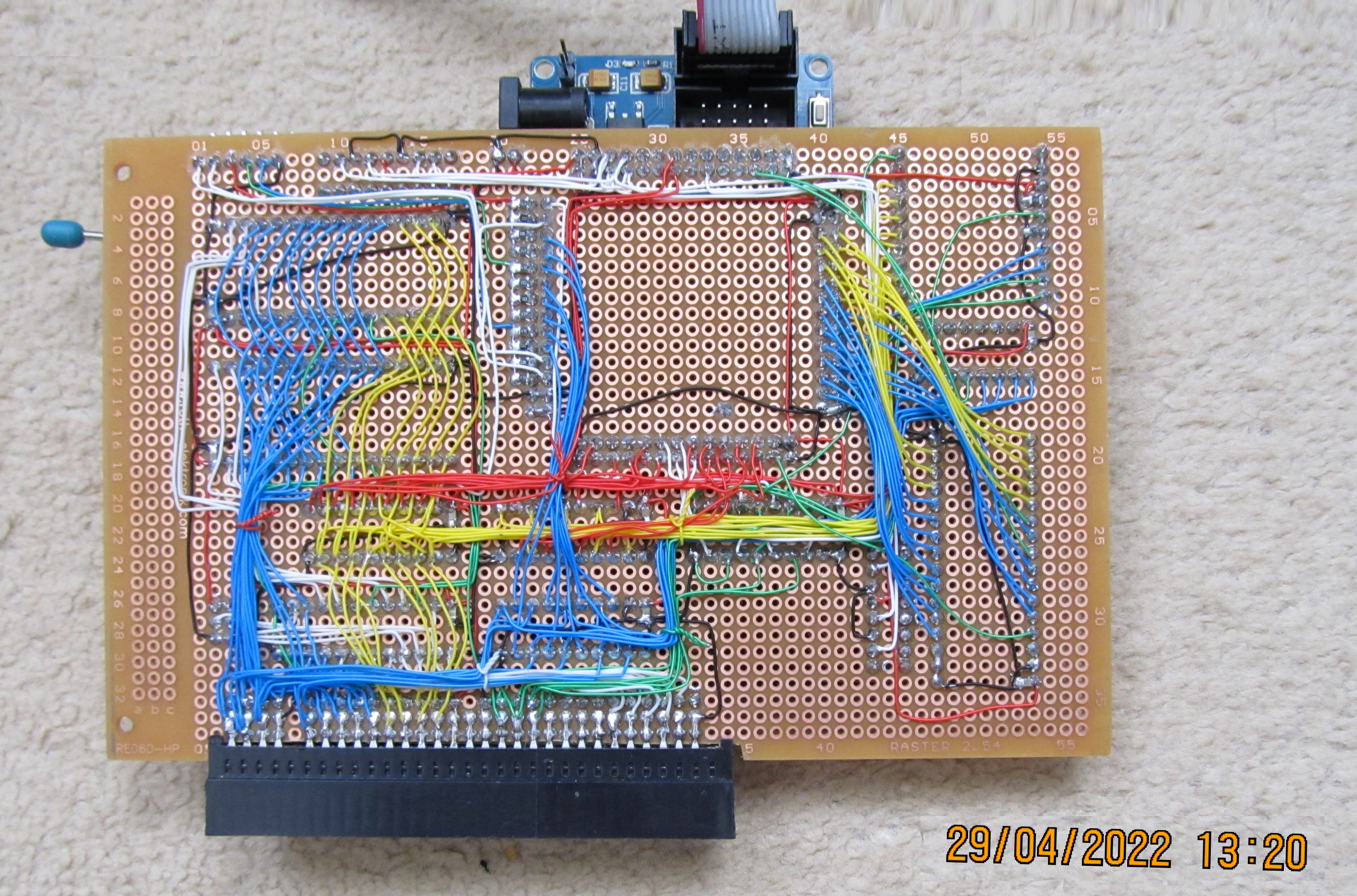
Martin's
prototype taking shape . . . .
The headers have
been mounted and the sockets for the DIP components
soldered in. Mating the board to the MTX computer board
provided further confirmation that there was enough
clearance between the components and the MTX I/O
connectors - including Martin's "special" video
connector. |
 |
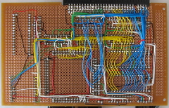
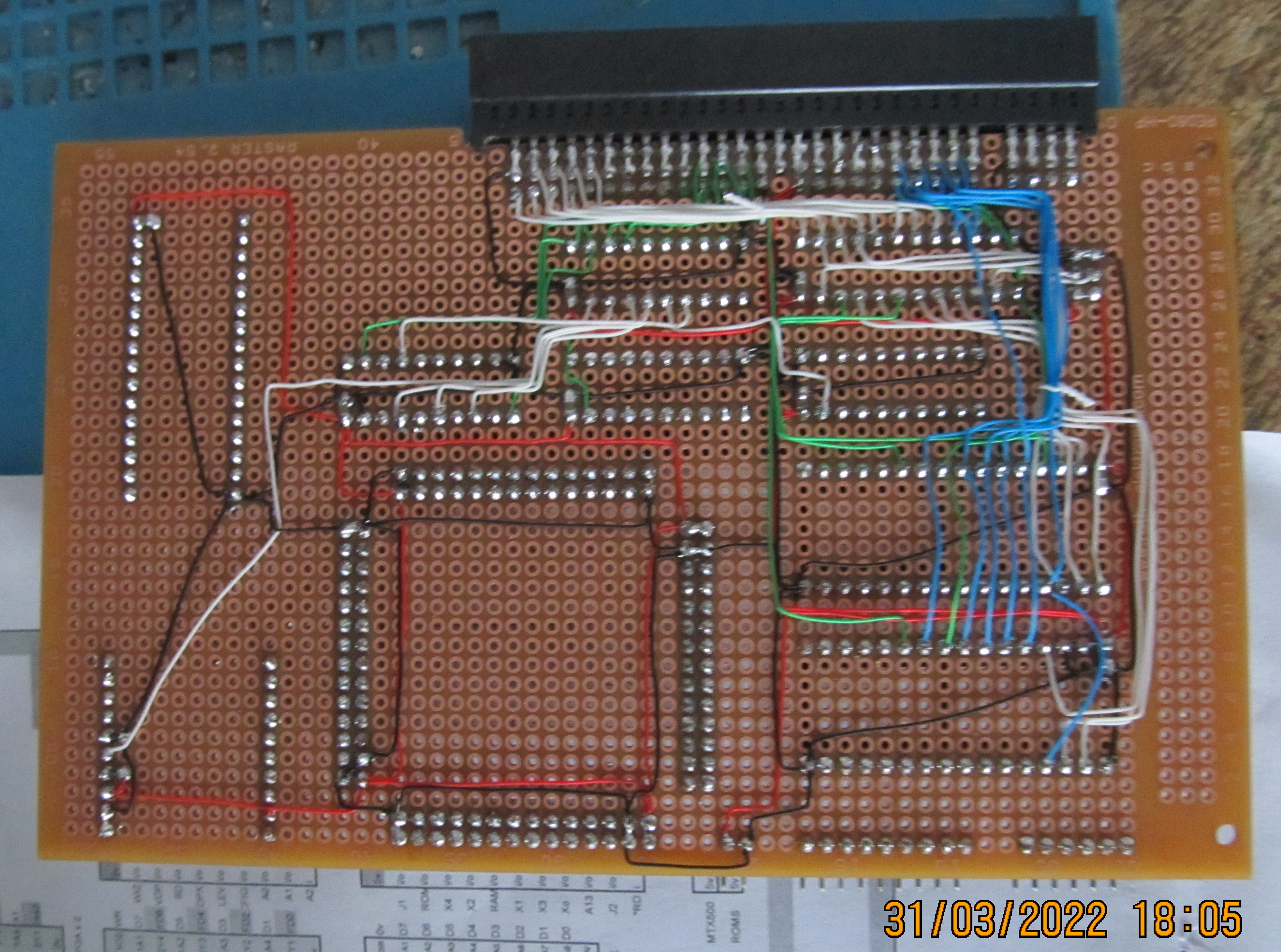
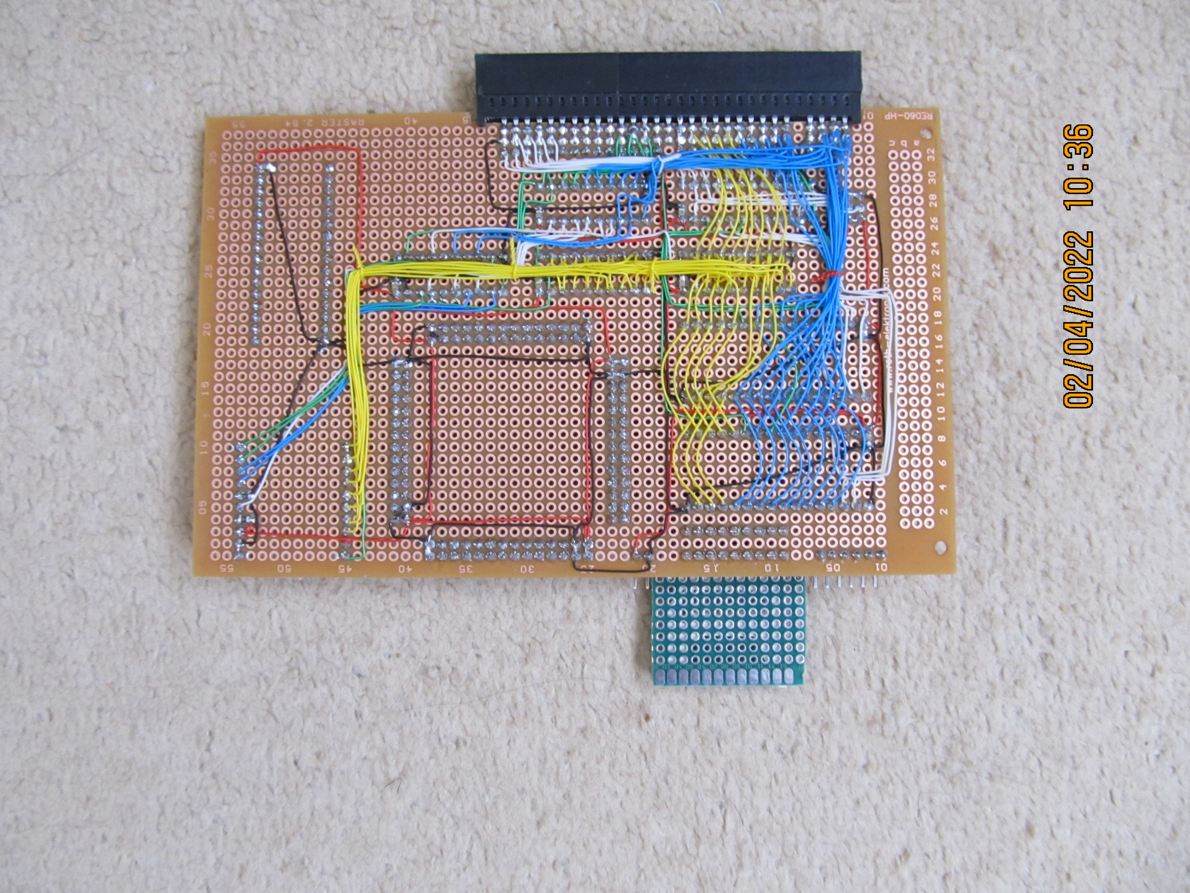
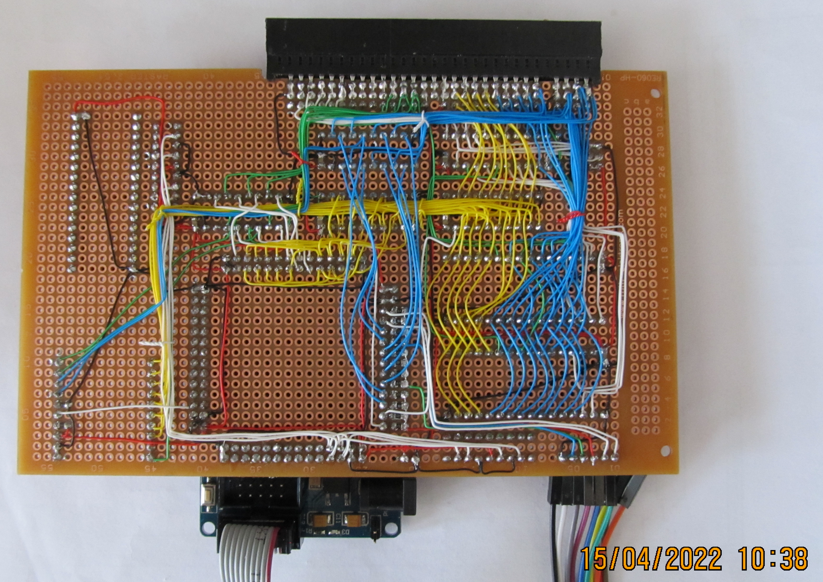
Solder
side of the proto board with the memory chips and GALs
about 50% wired - another example of Martin's excellent
prototyping skills!
Martin planned to ensure that
the ROM/RAM functionality was tested and working before
moving on to the FPGA etc. |
 |
For the
prototype, Martin chose to solder a bare SD card slot
onto a small piece of proto board, rather than use a
preassembled module.
This view shows the sockets
for the FPGA headers and DIP packages.
The jumpers are
to allow selection of the RAM area to be provided, i.e.,
whether the RAM is being used in a MTX500 or MTX512. |
 |
| Now with
the RAM and other, non-FPGA, connections fully wired,
ready to test paging of the extended RAM |
 |
The board
fitted, ready for testing.
As you can see, the SD
card has been repositioned to allow the board to be
fitted internally and a VGA connector has been connected
to the header pins. The VGA connector has been
positioned such that it is accessible through one of the
RS232 port cut-outs. Space on the Eurocard sized board
is getting tight - the production board may need to be
wider! |
 |
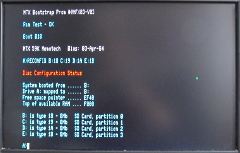
| Test of
the paging logic on a 64k MTX512. The MTX page port only
has 4 bits for the RAM page, so in BASIC there is the
base 64k + 14 pages of 32k from the 512k chip. With the
boot memory test needing a blank ½, page 15½ pages + 16k
common RAM is the maximum. The remaining 64k of the 512k
is unreachable. In CPM mode all of it should be visible |
 |
Whilst doing
some initial work on converting Andy's VHDL, Martin
realised that a minor design change was needed.
The I/O code linking the FPGA to the Z80 is controlled
by the CPU clock signal which was not buffered in the
initial MFX build. As there were no free pins, an extra
buffering chip was required and rather than decoding the
I/O ports on the board, the FPGA will have to do that
for itself (and the Wiznet)
That freed up the
16V8 GAL socket for a 3rd 74LVC244 instead. There would
then be one 244 for the data bus, one for the lower half
of the address bus, and one for control signals. That
actually had some advantages, the LVC244 is cheaper than
the GAL, doesn’t need programming, and looked to have
better availability. It would also allow the inclusion
of an emulated DART if FPGA resources permit.
|
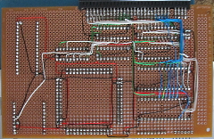
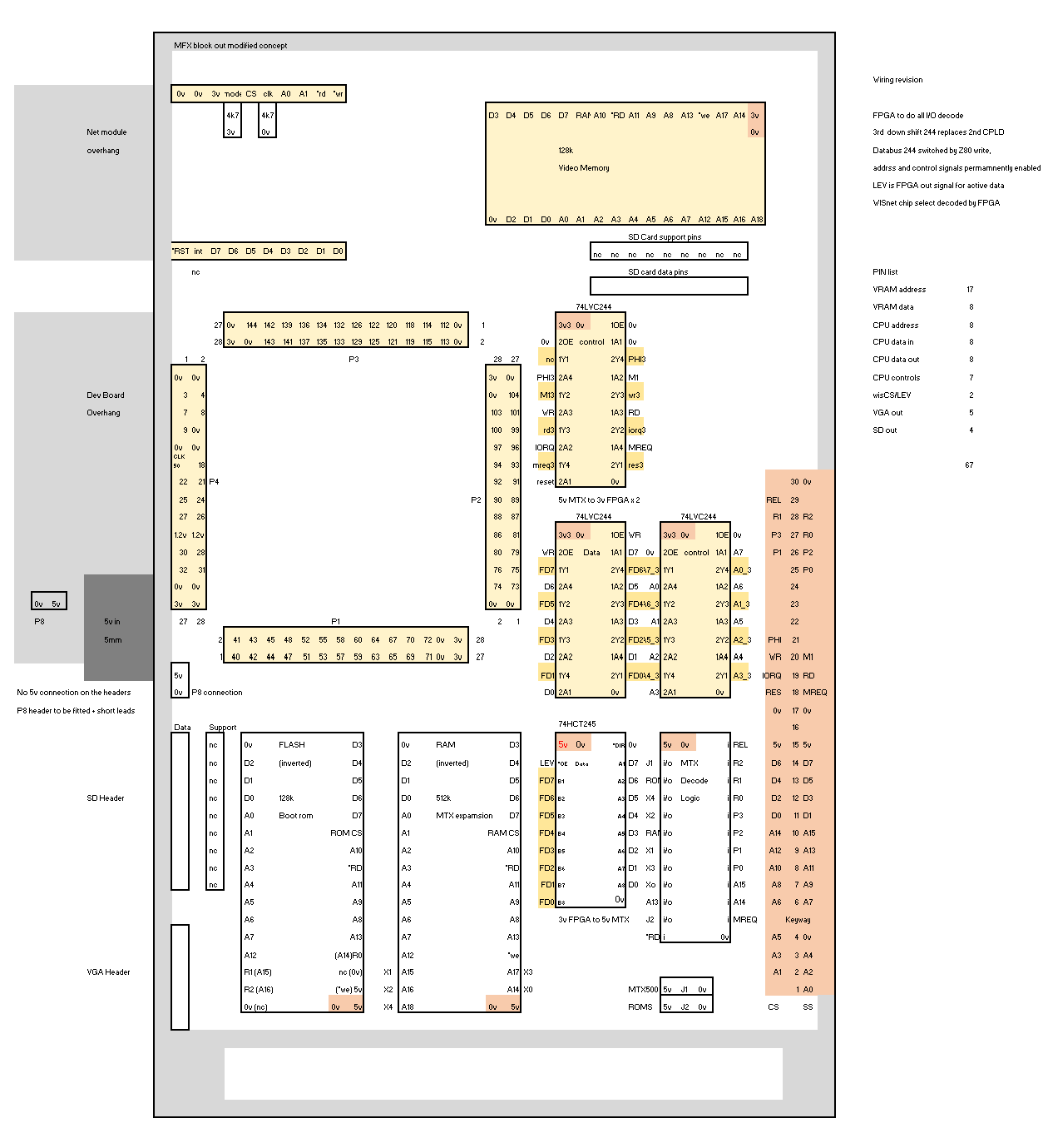
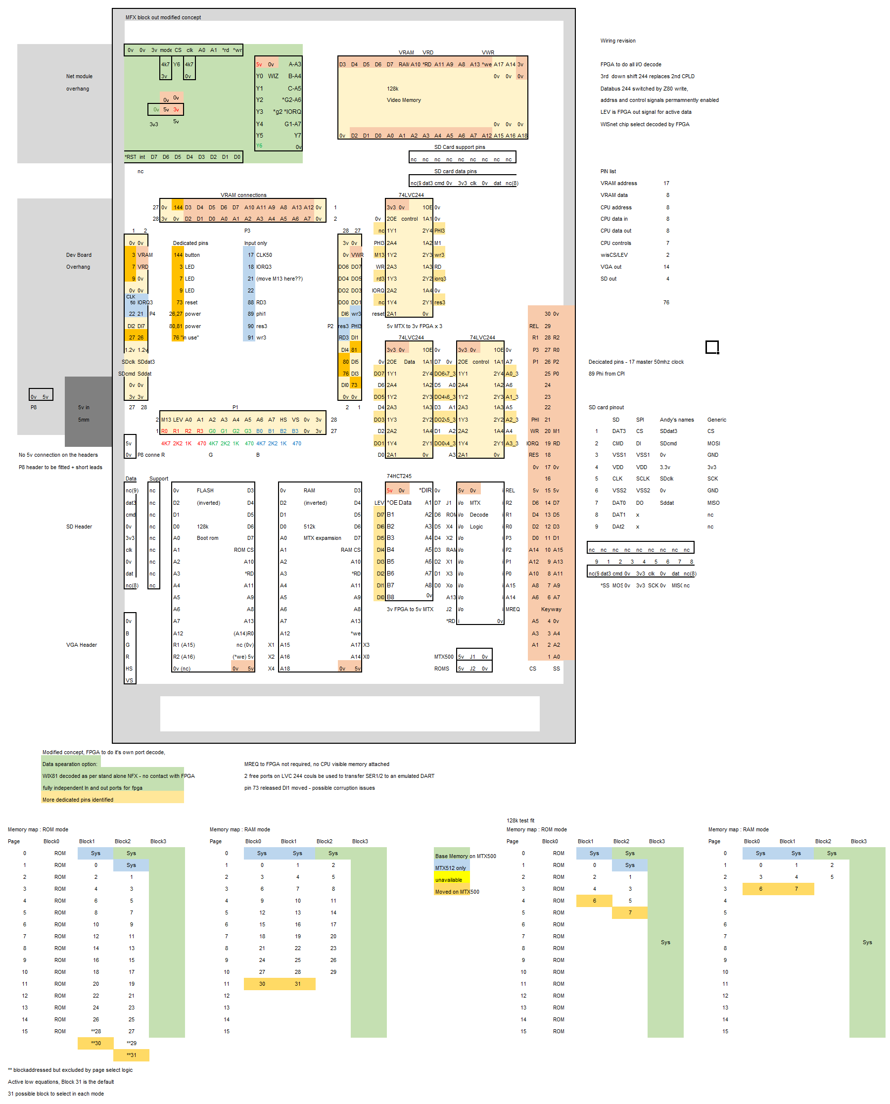
Martin's modified board arrangement.
From a
hardware perspective, things were looking good - at this
stage, a quick count of the FPGA pins required was 67
out of the available 89, but the availability of the
required logic resources (Logic
Elements) needed to be confirmed.
Andy's
VHDL for REMEMOTECH included emulation of the Z80 which
was obviously not required for MFX - the emulation of
the VDP was expected to be the most resource intensive
requirement and early tests has indicated that this was
not going to be an issue. |
 |
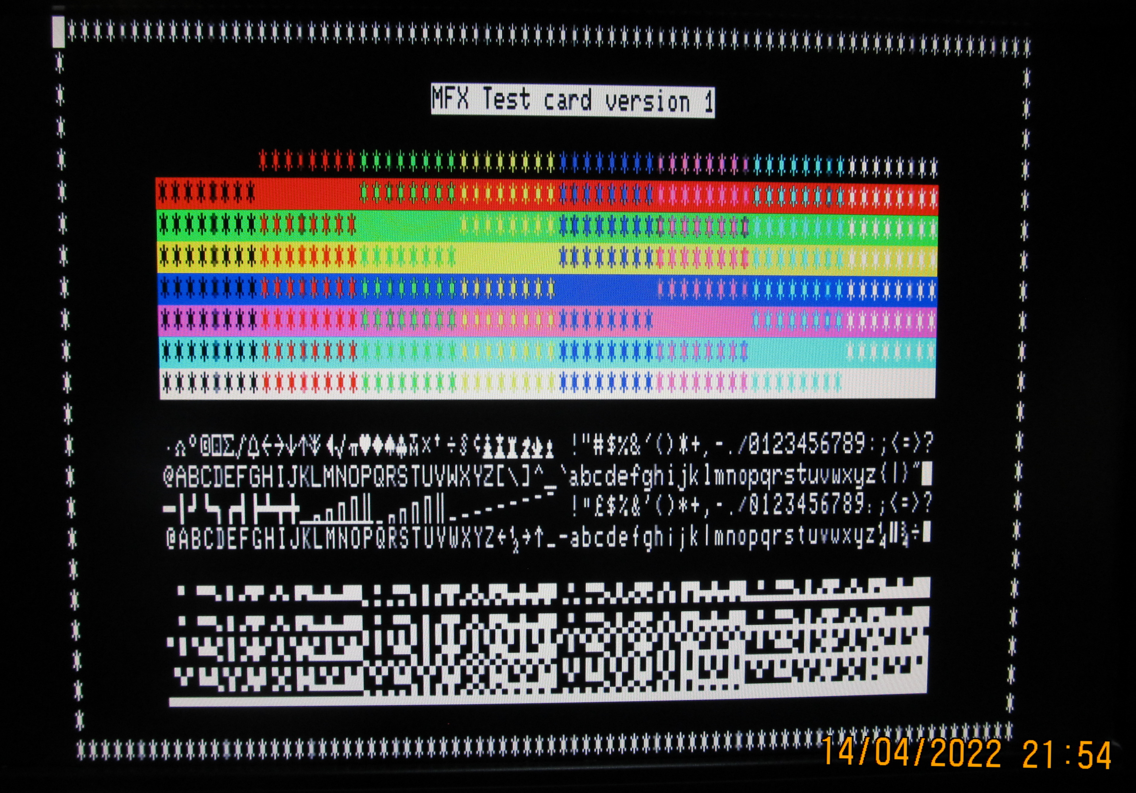
For
initial testing, Martin was running the board
independently of the MTX and concentrating on the video
emulation.
The video output from the FPGA was
seen to be "rock steady" - a very encouraging sign,
given, the issues seen with CFX-II.
The 80 column
Test Card graphic displayed on a VGA monitor. |
 |
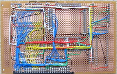
More
construction progress . . . . .
SD Card slot
connected and chips inserted |
 |
|
Solder/wiring side of the board |
 |
At this point, it's
worth noting some points from a conversation between
Bill and Martin on the video side. I have recorded them
here as others may find it as interesting as I do, it
is pertinent to the MFX design and gives an
interesting insight into how the development is
progressing . . . .
Bill
developed the VDP to VGA emulation used in
CFX-II and
commented that
Martin may run into "the same problem as [Bill] had with
the Propeller version, the difference in frame rate
between the VDP and VGA. As a result the VGA frames will
often be generated part way through a screen update. Not
much of a problem from BASIC but likely to produce
screen artifacts for games.
The ideal solution
is to double buffer the VGA output. Render VDP frames at
50Hz, synchronised with the VDP (you will need to
monitor VDPINT), but display frames at 60Hz. This means
that every sixth frame will be a duplicate, but each of
the displayed frame is clean. The Propeller had nowhere
near enough memory to do that, but if you have an FPGA
with additional RAM you may be able to do so.
Martin noted that
the development boards Cyclone II
EP2C5 has just under 5k logic
elements against 20k on the DE1's EP2C20.However the
on-board RAM definitely isn't big enough for the VDP,
meaning the VDP code will need additional tweaking to
use external memory. There's 13k RAM on the EP2C5 so my
initial thought was that was going to be 4k screen
memory, and 4k each for the alpha and graphic character
ROMs. Andy's code is actually using logic for both
character ROMs. Since the VDP won't ever fit into13k
RAM, I may recode the alpha ROM as a memory block, to
save logic resources if that means I can implement
additional features.
If I get the 80 column board
working properly, then I'll add in Andy's VDP emulation
using external SRAM. I haven't looked at the code in any
detail, but like CFX-II it will only be echoing the main
VDP. VDP interrupts and the status register will still
come from the VDP so update mismatch could be a problem.
Avoiding the screen jitter that's visible on some
monitors is the aim. Andy does have some 50/60 Hz
features in the existing code, but I'm not sure they
will be of any use. While I do have a spare pin to
monitor the INT signal, monitoring VDPINT would need at
least the CTC echoing as well. As there's no direct
connection I'd have to try and watch for a interrupt
address matching the one programmed into CTC channel 0.
I'm also not sure a SRAM large enough to double/triple
buffer the display would be fast enough.
MTX RAM
and ROM are controlled by a dedicated 22v10 GAL and are
already tested and working.
|
Martin
made some wiring mods to try to solve the problem of
getting data from the MTX to the FPGA.
The main
change here is the rewiring of the data bus to allow
separate path for data in and data out, i.e., re-wired
for fully independent read and write ports on the FPGA. |
 |
With the
VHDL updated to match the new layout and after a little
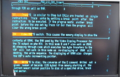
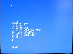
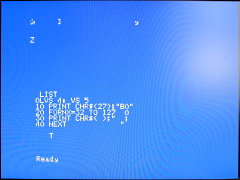
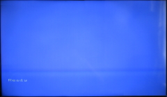
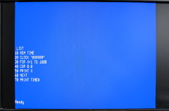
"tweaking", there is video output from the SDX boot ROM!
Despite being pretty garbled, you can make out
the text from the SDX boot screen which would normally
look
something like this. |
 |
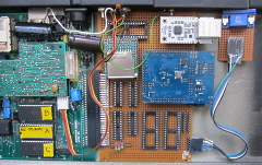
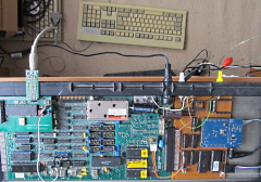
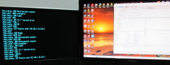
A photo of
Martin's test setup . . .
Really just an excuse
to promote the MTX to
PS/2 keyboard interface adapter that you can see
plugged into the MTX keyboard connector!
Here you
can see Martin's MTX connected to a PS/2 keyboard, which
as an added benefit in this case, allows the upper
portion of the MTX case to be completely removed for
testing. |
 |
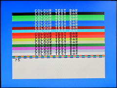
This image
shows the VGA output from the emulated 80 column card
when controlling it from SDX BASIC, by sending values to
the emulated ports for the display generator.
Writing to the ports as shown below allowed Martin to
display the output from the character ROM and set the
color attributes as expected. |
 |
For the 80
column card :
Ports 48 (30h) and 49
(31h) select the memory address
Port 50
(32h) selects the character in the the alpha or graphics
ROM
Port 51 (33h) controls the attribute
byte
With the output being as expected, this
suggested that the SDX ROM display corruption could
possibly be timing
related. |
 |
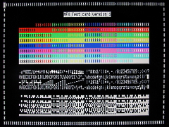
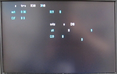
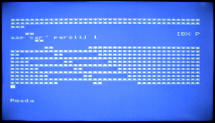
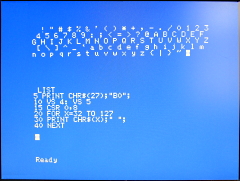
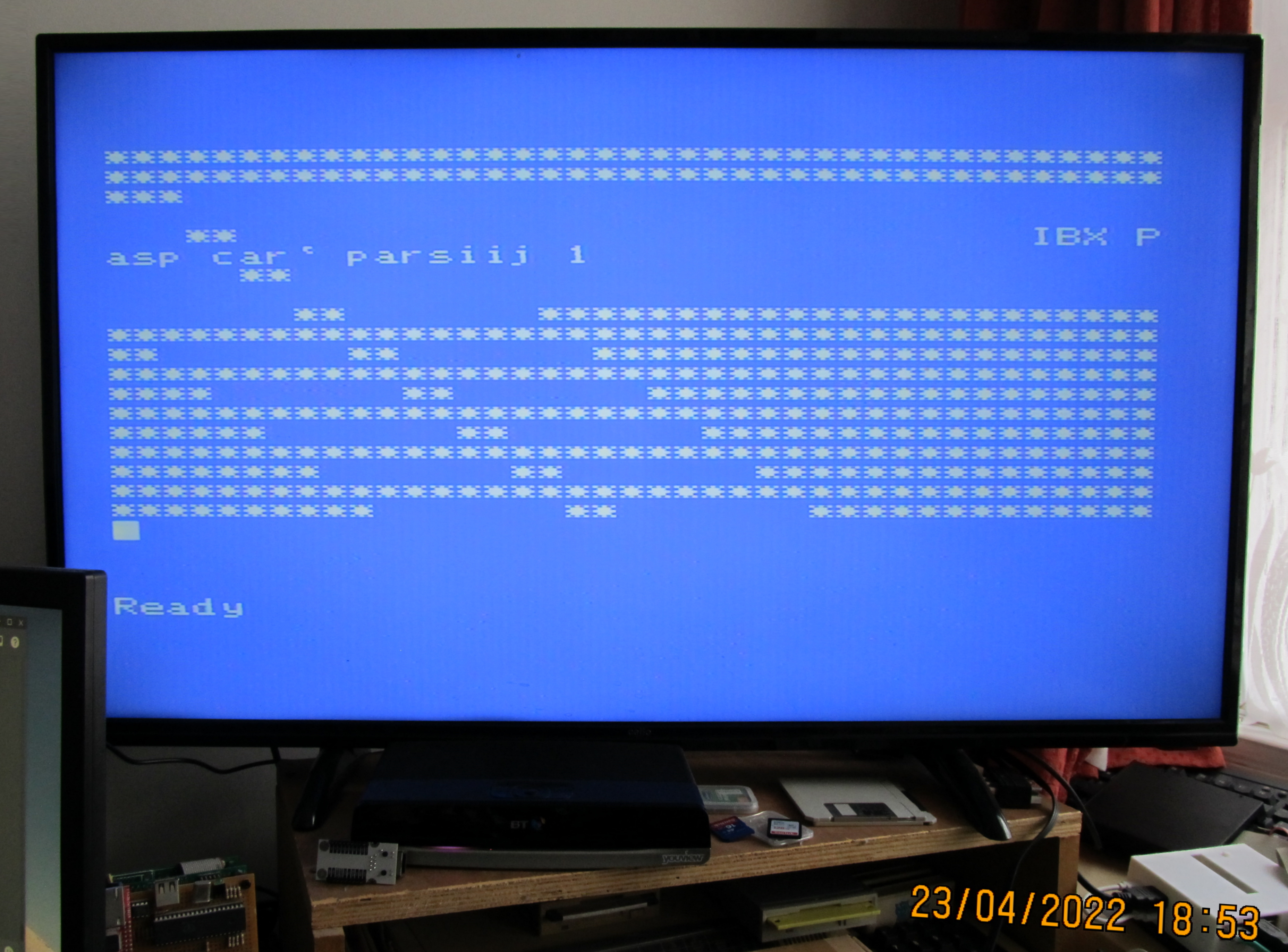
Reading
data back from the Testcard display helped identify the
issue.
Here you can see The “MFX Test card
version 1” text being read back and displayed as "IBX
Pasp car' parsiij 1". Looking at the ASCII codes
revealed that there was corruption of bits 1 and 2. |
 |
The issue
turned out to be caused by the way that the development
board dedicates some pins to allow for an external reset
signal and has pull-ups/downs on some pins that are
provided for if the board uses an EP2C8, rather than an
EP2C5 Cyclone II which is typically installed.
Reassigning the D1, D2 and D7 data bus signals made
a difference - there are a couple of issues, the green "
should be a space and the RAM data is actually from the
ROM - but this is great progress. |
 |
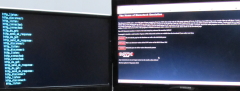
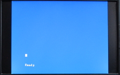
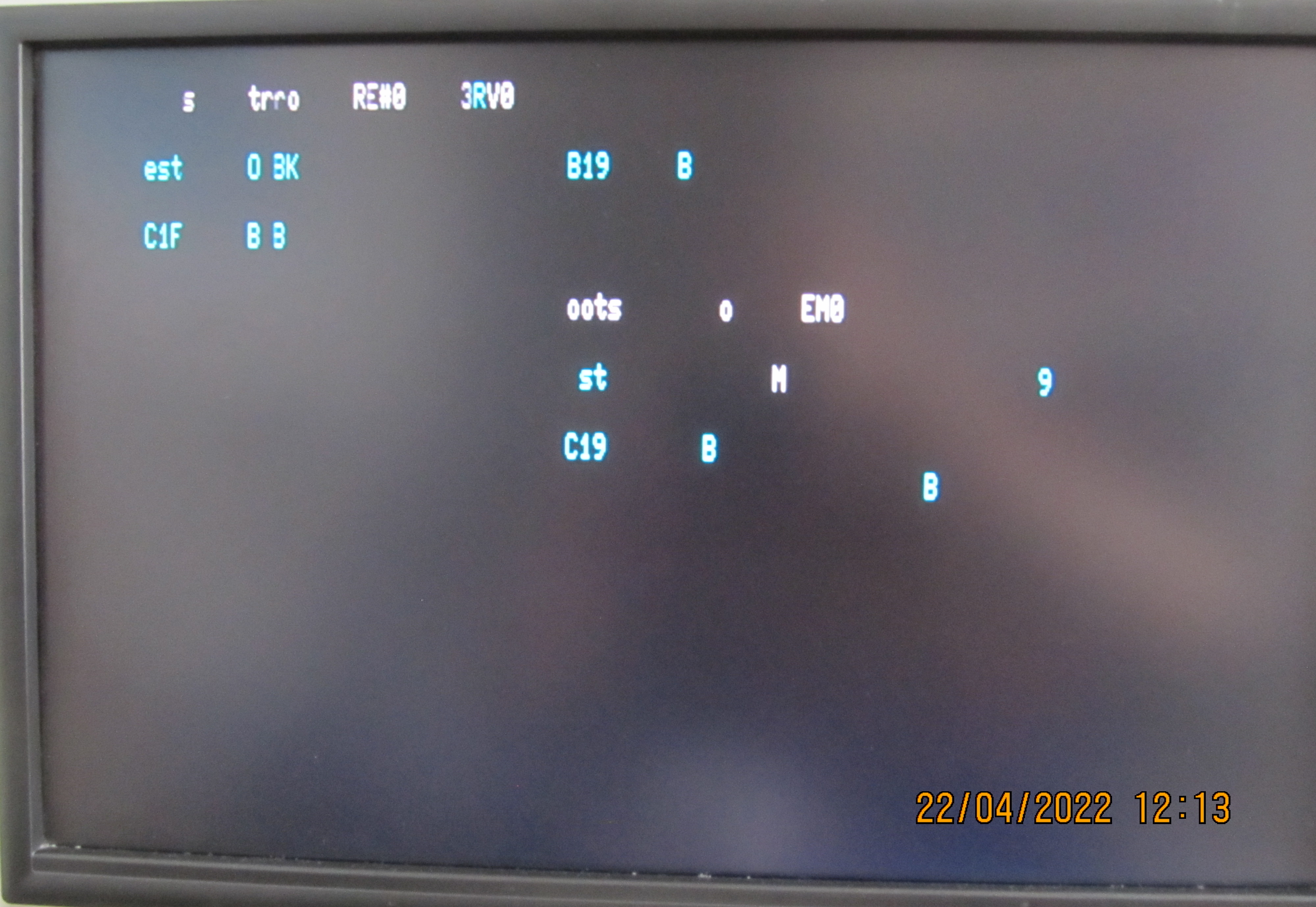
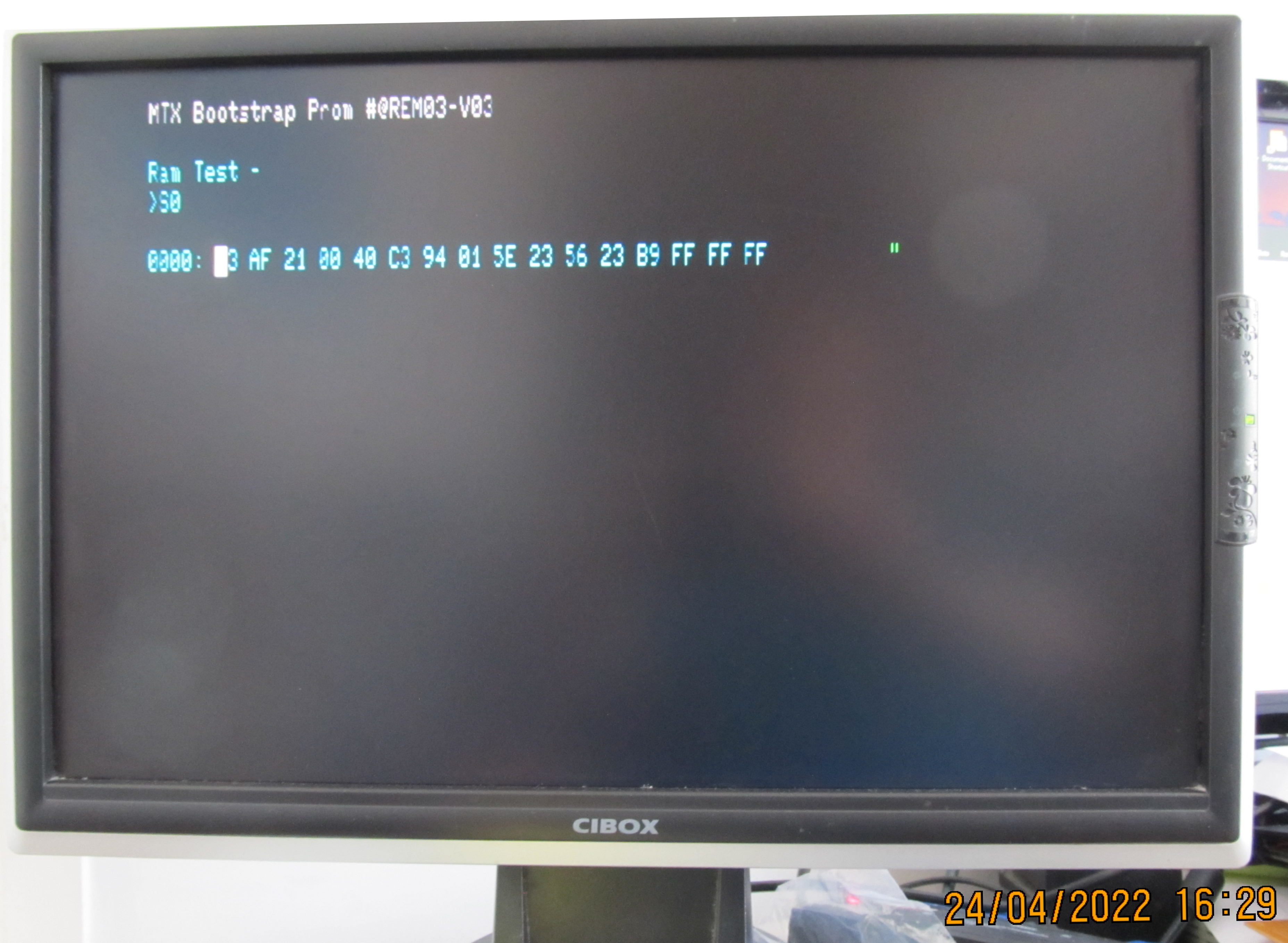
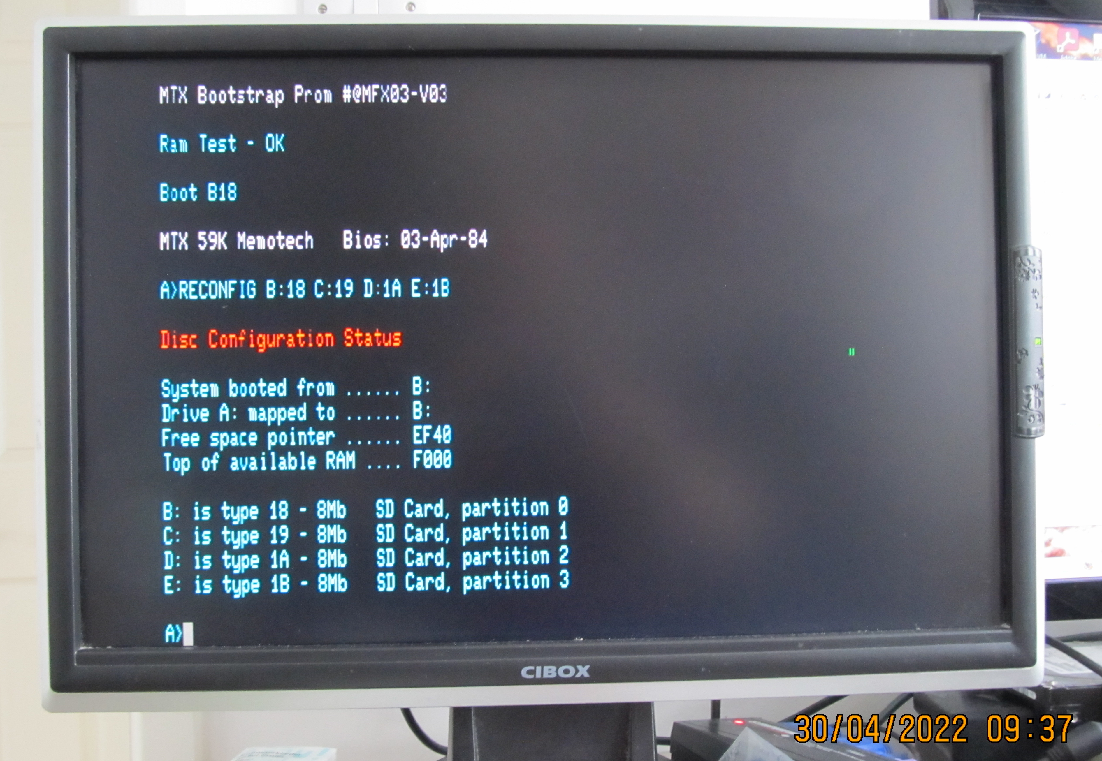
The data
coming from ROM, rather than RAM, suggested that there
could be an issue with the paging logic. However, the
MTX being used for testing had a history of issues, so
Martin tried a known good MTX.
As you can see
here, the RAM test was now "OK" and the system tried to
boot and read the startup string from the SD card. There
are still issues, but progress was being made! |
 |
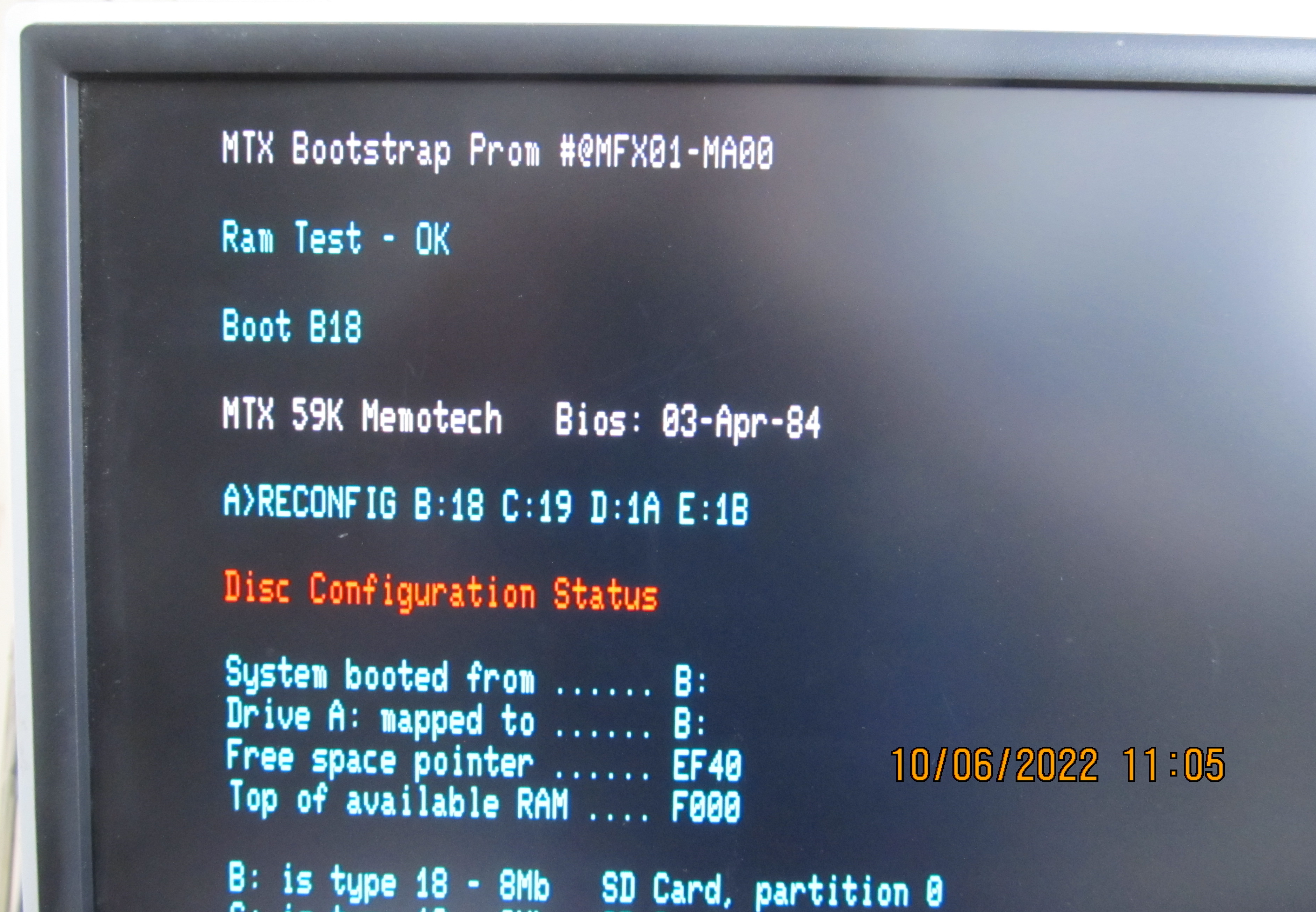
With the
system at least reading the SD card, Martin concluded
that the SD access part was fine, particularly as Andy’s
SD code was unchanged and it was all synchronised to the
FPGA clock.
It appeared that it was I/O
transfers to or from the FPGA that was being corrupted
in some way. To display the boot message, it must have
read at least 2 sectors from the right place – the
boot sector and the bios sector with the text shown in
the above image.
Martin updated the wiring "schematic" with colour coding
for the "reserved" pins on the FGPA board.
(The
reserved I/O pins reduce those available for MFX use.
Whilst not ideal, it would be possible to make these
pins available by removing the associated
pull-up/pull-down resistors on the FPGA board should it
be necessary. This would require minor modification to
every development board which is obviously not something
that we'd want to do.)
|
 |
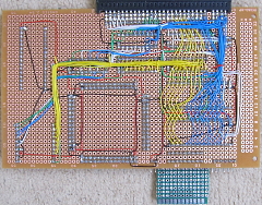
Updated
prototype wiring.
The the SRAM chip intended for
video memory wired up.
In addition, a 138
decoder has been added for the Wiznet to make it totally
independent of the FPGA for testing. One advantage of
that is that this way has already been proven to work on
NFX. |
 |
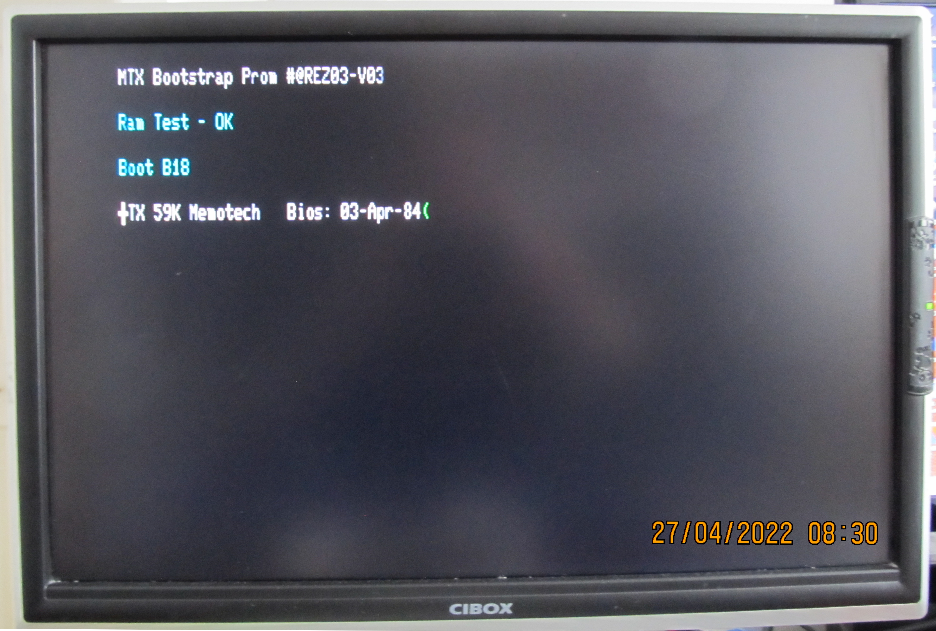
Looking
good !
With some minor optimisation of the VHDL
code, here you can see the system booted from the SD
card and running CP/M!
You can see one small
"glitch" on the screen and intermittent data errors
meant that booting sometimes failed, but things were
looking good ! |
 |
One significant
difference between ReMemotech and MFX is the requirement
for level shifting between the 5v MTX and the 3v FPGA.
The external buffer for the FPGA outputs needs to be
turned on when needed and the 74HCT245 had a typical
cycle time of 20ns - the same as the 50MHz FPGA, so the
buffer could potentially have been a whole cycle behind
the FPGA.
In an attempt to speed up the
transfer, Martin replaced the HCT part with a faster
74F245 which produced some improvement.
|
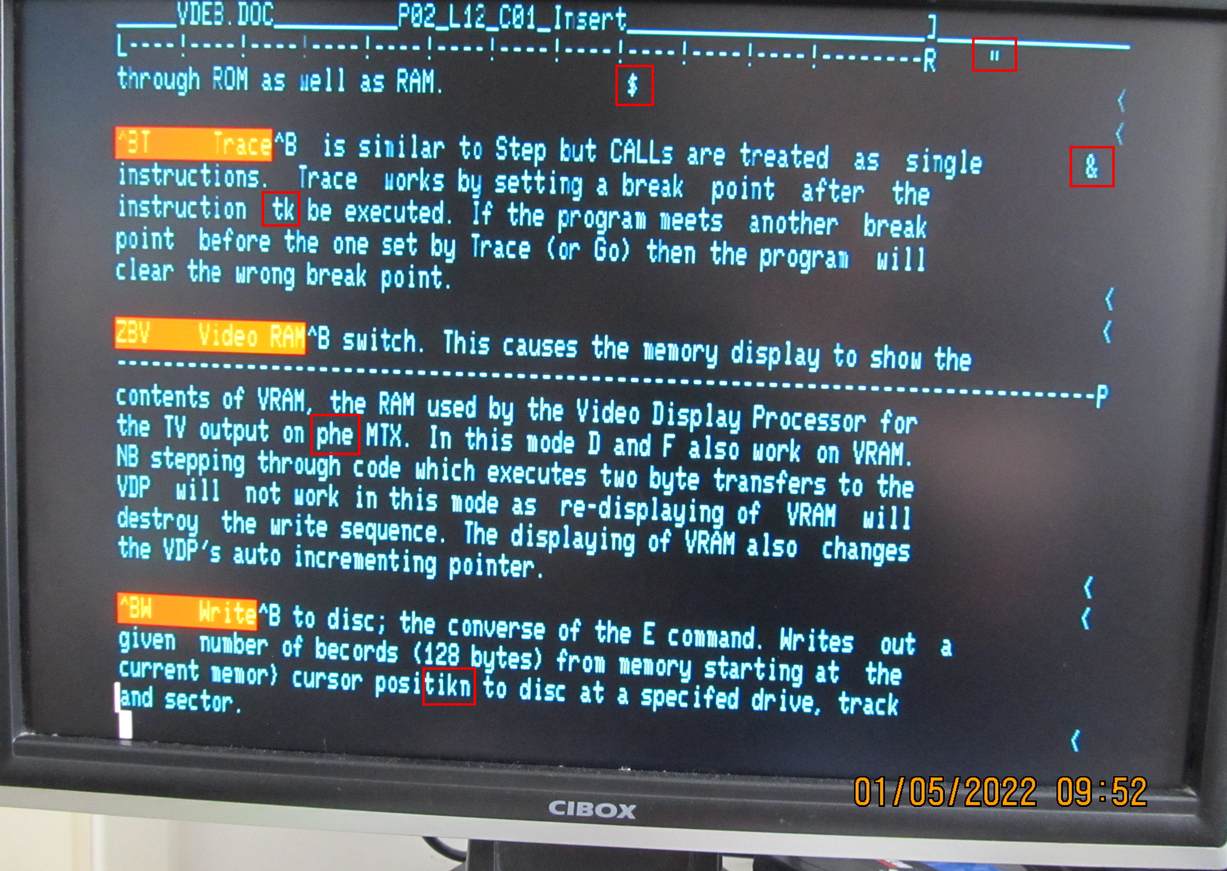
Whereas
previously NewWord would not successfully load, this
screen shot shows NewWord has loaded and is displaying a
document when the faster buffer was used.
The
issue has not been completely resolved - there are a few
character errors which be seen in more detail by opening
the full size image. If the issues are down to switching
speed, then it is possible that an even faster buffer
may help, alternatively, it could be a "noise" issue. |
 |
With the F245 parts
having apparently made some improvement, Martin decided
to try an even faster part - a 74AHCT245. These
(A=Advanced ) parts, unlike the "F" family are CMOS,
have the right output specs, and are a fraction faster
as a bonus.
In an attempt to reduce any "noise",
Martin also planned to install some resistors on the
data lines.
|
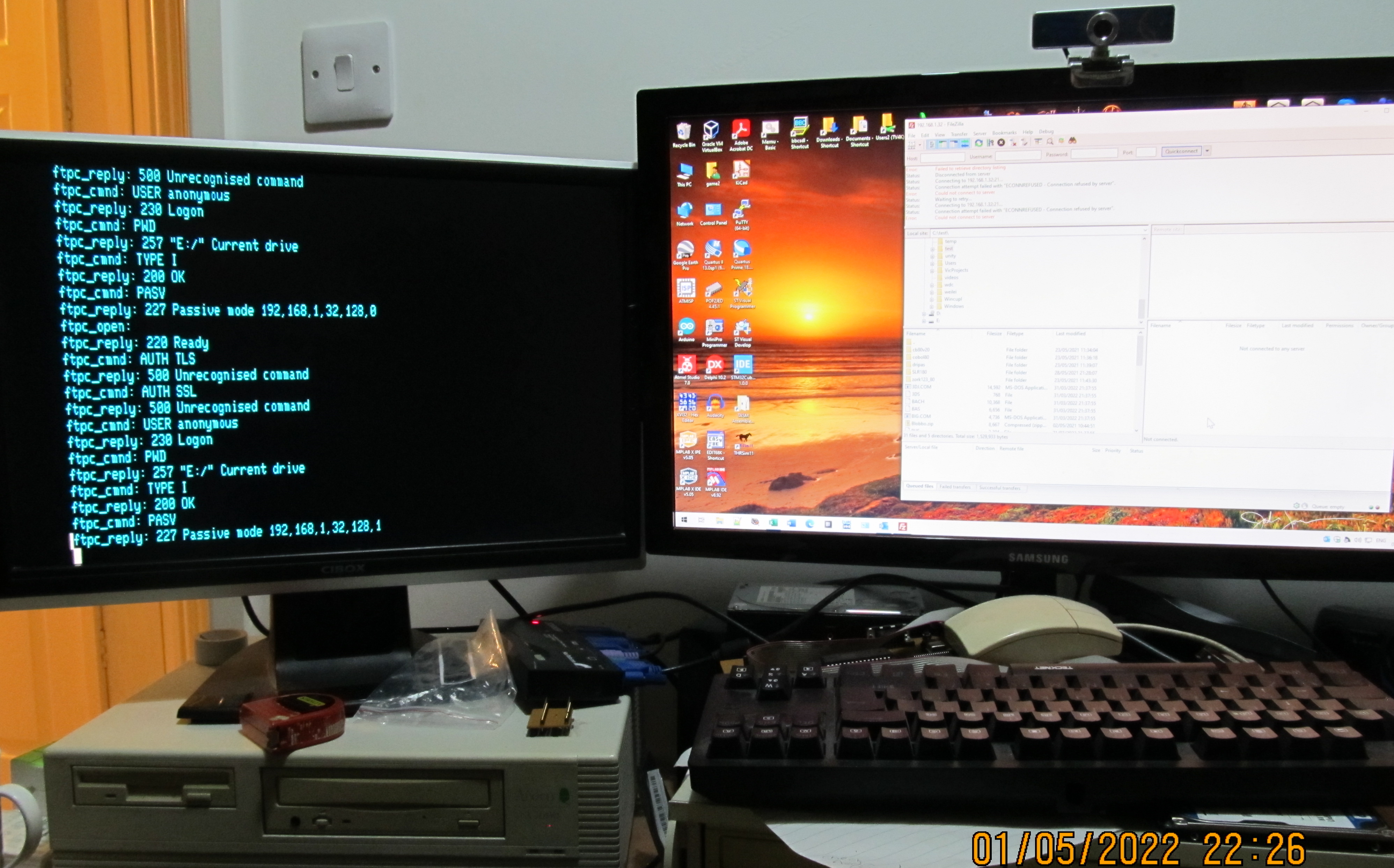
With
"noise" in mind, in order to cut down the amount of
unterminated wiring on the board, Martin connected up
the Wiznet adapter. After correcting a minor wiring
error on the enable signal, the NFX programs for
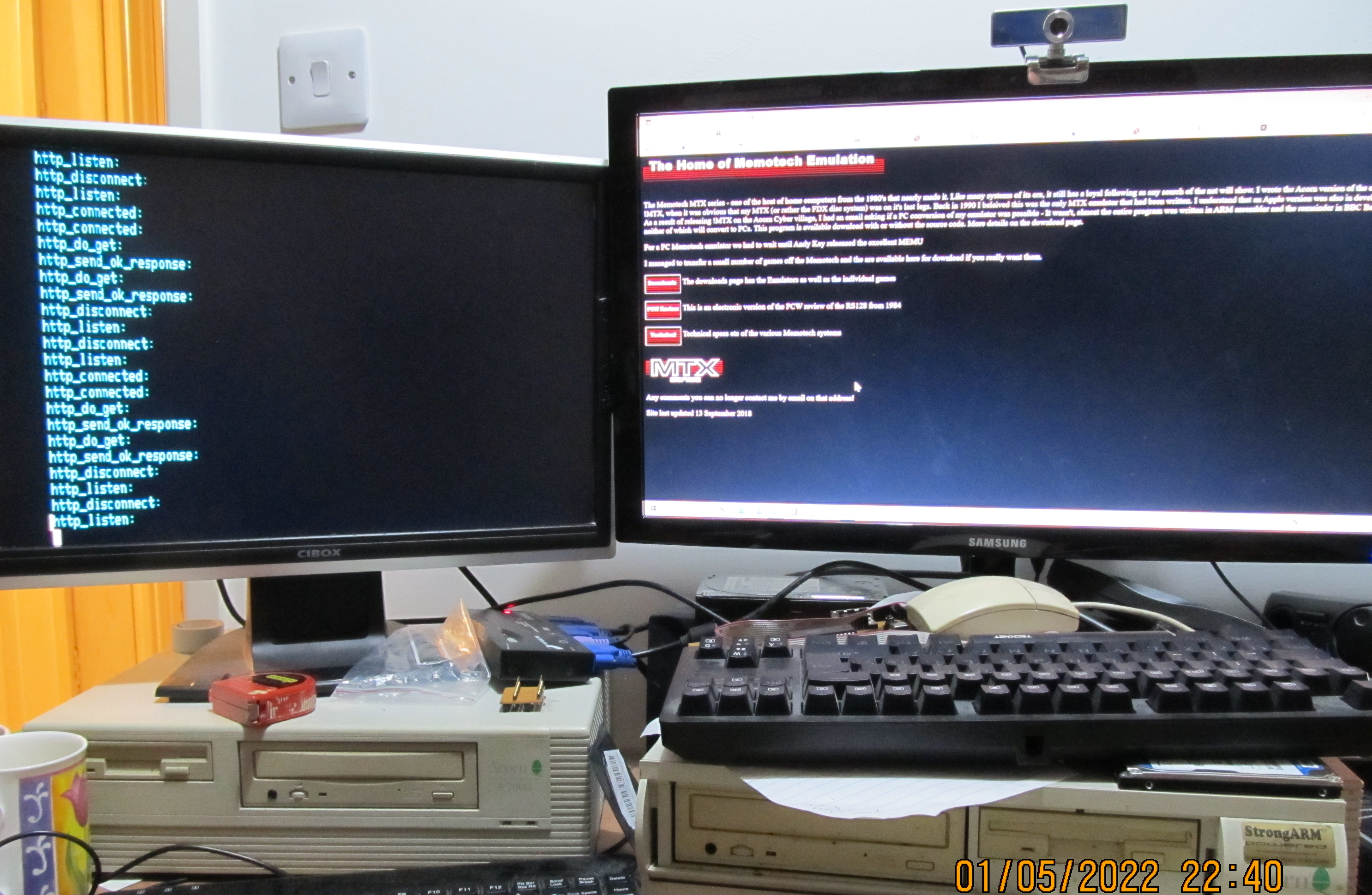
FTP and HTTP were proven to be working.
With the
Wiznet adapter connected, there appeared to be less
screen corruption and accessing the SD card appeared to
generate fewer errors. However, there were occasional
dropped connections to the Windows FTP server, possibly
supporting the belief that there were noise issues. |
 |
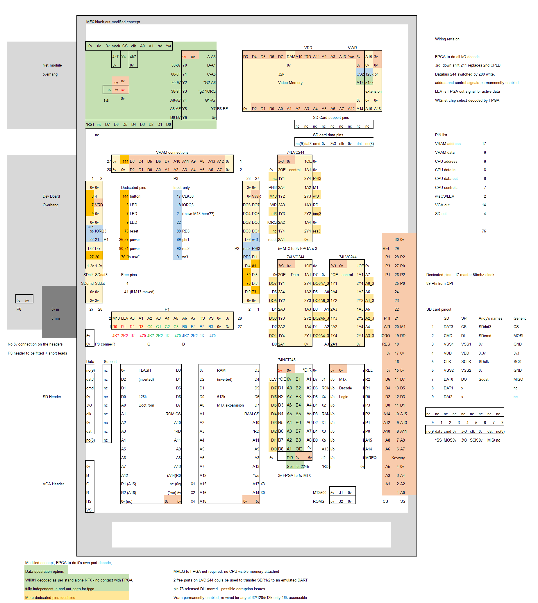
Updated
wiring map with minor changes, including
Correction to the Wiznet enable signal
VRAM always enabled
VRAM socket wired
for 32k/128k or 512k RAM chips
(although only 16k currently enabled)
With the
hardware wired, Martin could then move on to looking at
the VDP, starting with the import of Andy's VHDL code.
Some changes were needed as the original assumed 20ns
dual ported RAM and that the system could read/write its
VRAM at will., whereas MFX was using 55ns single port
RAM.
Having the CPU side write only was an
advantage, the host VDP would respond to reads, so
the emulated VDP didn't have to. CPU writes could be
directed to a 1 byte buffer to be transferred when the
state machine had time. (This may be how the real VDP
works without the luxury of dual port memory.) The now
redundant code to do with VDP interrupts and the status
register was also be removed. |
 |
Martin observed
that the extra “activity” in the FPGA also made the SD
and 80 column a little more unreliable.
The
faster '245s arrived and were fitted, but had no
noticeable impact on the occasional 80 column card
output glitches and the SD card reliability, but work
continued on the VDP emulation code.
(Once the
real problems were diagnosed and resolved as described
later, the replacement '245 level shifters were removed
and the standard HCT versions were reinstated. The AHCT
version's extra transition speed comes with its own
problems with ringing, an unnecessary complication which
could be avoided.). |
Initially,
it was text mode only while Martin dealt with the
complications of single port RAM. Andy’s code takes
advantage of the speed of the local RAM to do all the
sprite processing in the horizontal blanking period.
Martin couldn't do that as not only is the SRAM a lot
slower, access also needed to be shared between the VDP
and the CPU.
Although not quite "Ready”, the
output was definitely recognisable. The obvious
corruption issues were down to missed writes (since the
real VDP deals with the reads). |
 |
Understanding why
some writes were being missed required some thought. In
Martin's words . . . . . . .
The FPGA clock runs as 50Mhz,
so each step of a process takes a minimum of 20ns.
That’s the master clock for the SD card and the memory.
The internal memory works in 1 cycle, the external needs
3 and I’m currently using 4 to guarantee some division
between read and write.
The VGA clock runs at 25Mhz,
so has a cycle time of 40ns. Each line is approx. 32us
made up of 800 clocks 640 active screen area 160 blank.
Andy’s code does all the sprite processing in the blank
area.
The pixel clock for the VDP output is half
that of the VGA clock (12.5Mhz) because it’s only 256
pixels wide plus the VDP border to fill the rest. That
means - theoretically - there’s time to access the VRAM
on every pixel displayed. For text mode, only 2 reads
per character are needed. Read the character code and
then read the pixel data for the current row of that
character.
The CPU clock is 4Mhz, 250ns cycle
time. I/O port. It’s not synchronised to the FPGA clock.
But the ROM code does honour the VDP data sheet in that
VDP writes in text mode are no closer than 8 CPU cycles
and in G2 mode 32 cycles.
It should be easy to
satisfy those timings. 8 CPU cycles is 2000ns that 25
VDP pixels. So fitting one CPU VRAM access slot for each
character position (6 or 8 pixels depending on the
mode). Should be more than enough.
[The previous]
screen shot was taken with the CPU having 2 slots per
character. And there are missed transfers. There must be
something else affecting the transfers other than just
the memory access slots.
It may be that solving
that helps solve the problem with the other I/O. My
biggest concern initially was the lack of
synchronisation. The start and end of the CPU I/O cycles
will never match the FPGA clock, so potentially the
could be really small part cycles at the ends as the
FPGA views things.
The other issue is the signals
pass through 3 different down shifters. Is possible they
won’t have exactly the same response times. So on a
“runt” cycle some signals might still be changing when
the FPGA starts processing the input. Noise on the bus
could produce the same result.
One of [the]
“tweaks” was to only accept an I/O request if it was
active for 2 consecutive cycles, which would hopefully
eliminate both noise, and part cycles. But alas, it
didn’t solve the problem (yet). |
At this
point, the VHDL as written, had the possibility of
writing to an I/O port more than once. This would not
have been a problem if it wrote the same data each time.
However, since the clocks aren’t synchronised, this was
likely not to be the case.
Martin stopped any
early access being part formed and causing corruption,
but also needed to put a stop any duplicate accesses and
see if that improved things further. |
 |
A complete
re-writing of the handling of the I/O ports used by the
VDP was done. Martin needed to account for the VDP worst
case 15 (of 16) VGA pixels/cycles between the CPU
issuing a write, and the VDP having the capacity to
action it. - The VDP text display was now flawless!
The re-done code stopped any IO ports being written
twice because the CPU is relatively slow compared to the
FPGA. (The 80 column board and SD card ports I/O
handling would be moved over to the same system to see
if that cured the glitches there.) |
 |
The text
part of Graphics Mode 2 was also working.
Graphics Mode 1 was probably working to, the code ws 80%
the same a G2 mode, but not tested at this point.
Until the SD card R/W was working properly, there
was no way of testing it. Work on the sprite engine was
the next step . . . . |
 |
A sprite
test screen. There was some horizontal flicker, which
appeared to be interference between the sprite engine
and the regular SRAM access sequence.
Martin
commented I need to track
down the cause as Andy’s source indicates that the
sprite stuff should only be active in the vertical
blank.
To
get round the sprite engine needing a total re-write for
single port RAM, I invented a work around. I have one
free SRAM access cycle per character cell per row. 384
(192 lines doubled) rows x 32 cells is more than enough
to copy a the 2k block of sprite patterns and 128 bytes
of attributes to dual port RAM. The sprite engine can
then run from the on-board DP RAM at full speed and I’ll
only need to edit a few pointers. The initial work is
promising there is something getting output. I did
manage to confirm it wasn’t the SRAM to DP RAM copy
causing those glitches. |
 |
Progress
of the sprite processing logic . . .
The upper
image is the output from the MTX VDP and the lower image
is the corresponding image being output to VGA from the
FPGA. Though not visible on the images here, there was
still a little corruption of the FPGA sprite images.
Parking that issue for the moment, Martin spent some
time investigating the corruption in reading data from
the SD card. . . . |
 |
To get a feel of
what was going on, he used PANEL
to compare the data read from the CP/M tracks by the SDX
ROM with that read by REMEMOTECH.
Having scanned
through 400 bytes or so, he found 5 errors, and all 5
were bit 7 being mis-read, both high and low.
As
you may recall from above, in order to cater for the
board's dedicated I/O pins, the FPGA to CPU D2 and D7
connections were previously moved to the other side of
the FPGA which may have had an effect.
To
eliminate that as the cause, he moved the D2 and D7
connections to the same bank as the other data bits, and
having seen no improvement, Martin put his 'scope on the
data to check the signal quality.
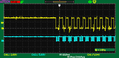
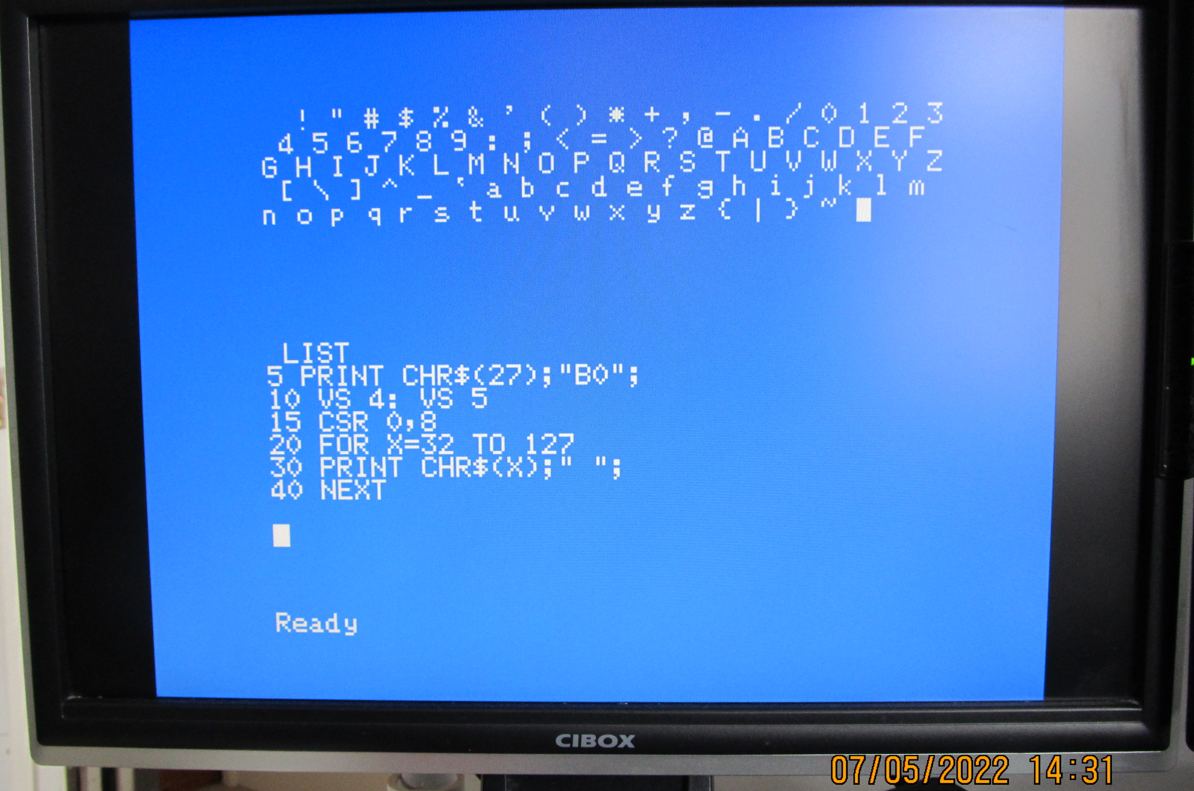
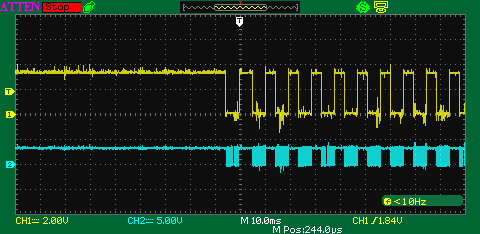
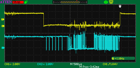
|
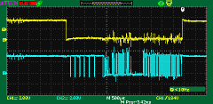
The yellow
trace is the chip select, the blue is data. The scope
was triggering on the first time SD select drops after
reset, so in theory it’s doing the low speed device
setup before moving to the 25mhz of flat out transfers.
In the upper image, with a relatively slow time base
(10ms/div), you can see that the 0v level of the select
signal is showing some pretty large spikes some
exceeding a volt. The data doesn’t look as bad until you
zoom in.
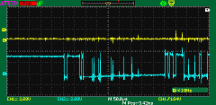
In the middle image, at 500us/div,
there is lots of noise apparent on the chip select line
and the data looks somewhat messy too.
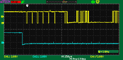
The the
third image, with an even faster time-base (50us/div),
you can see that the signal appears to have some
horrible spikes all over. With this level of noise, it
is probably unsurprising that some data corruption is
occurring! |
 |
Martin
added some 100nF capacitors to the WIZnet and SD card
headers and removed the duplicate SD card header wiring.
In this trace, blue is select and yellow the data
with a time-base of 250us/div. The data is now very
clean - Martin believed that removing the wires and the
spare header probably did most of that. |
 |
As well as
the minor hardware changes, Martin made more changes to
the VHDL that should hopefully remove any runt signals
from the FPGA if the CPU and VGA clocks happened to be
particularly badly aligned.
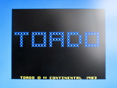
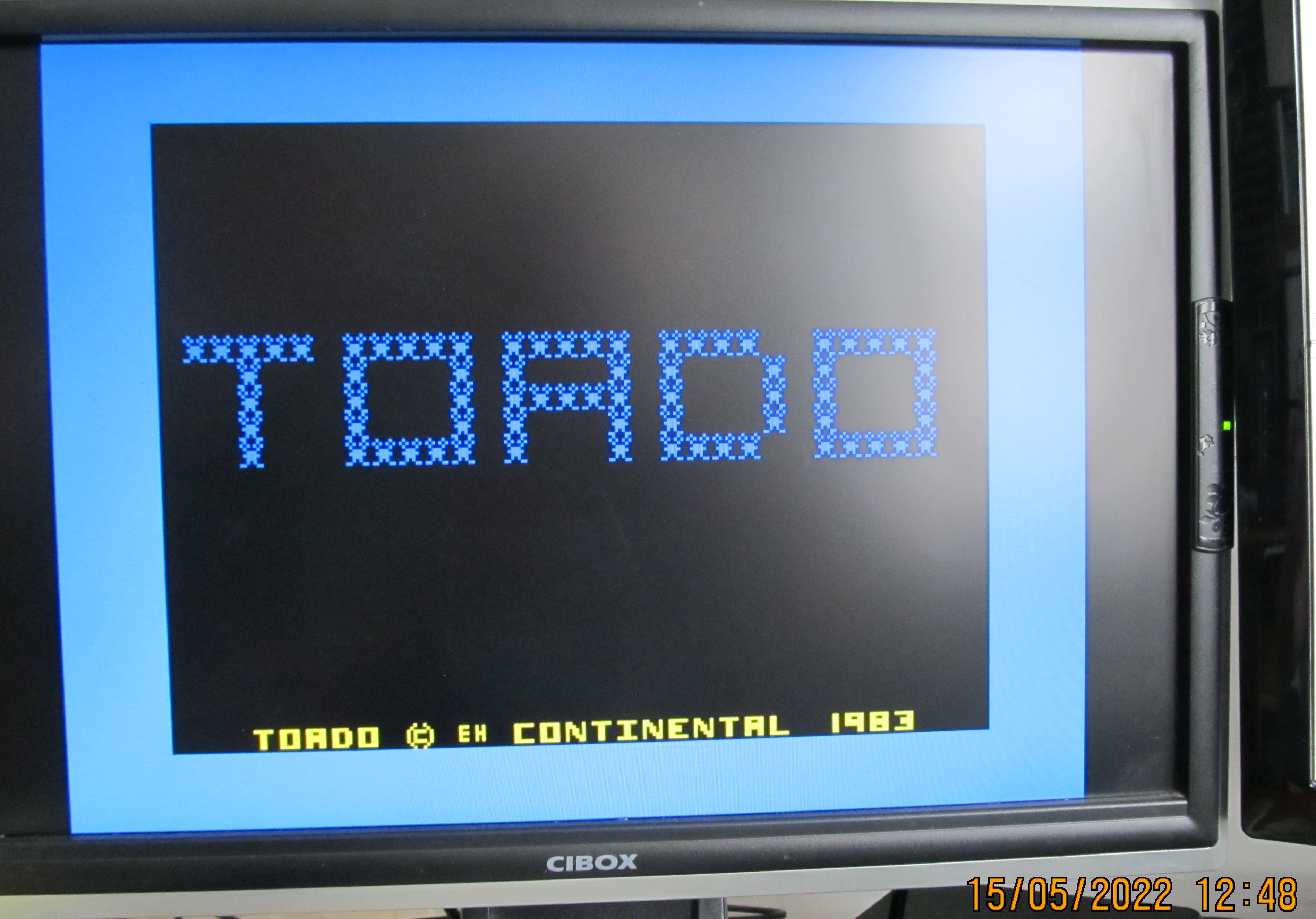
There was a marked
improvement. Here you can see Toado having loaded
successfully from the SD card, and . . . . |
 |
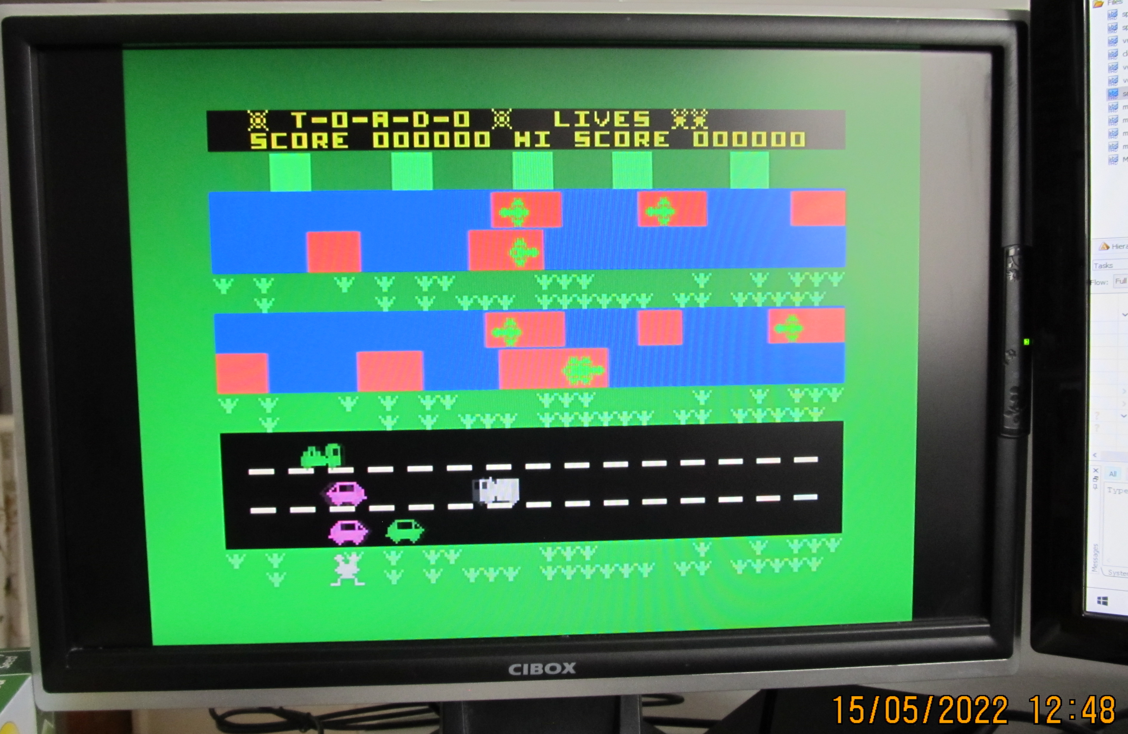
. . .
happily running and displaying its sprites on the VGA
monitor.
This is probably a milestone moment!
Martin had observed the occasional "flicker", likely
sprite related, but felt that a little code optimisation
would probably resolve it.
It seemed that as a
proof of concept, the MFX project to date had been a
success and confidence that an eventual product would
result was HIGH ! |
 |
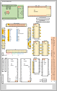
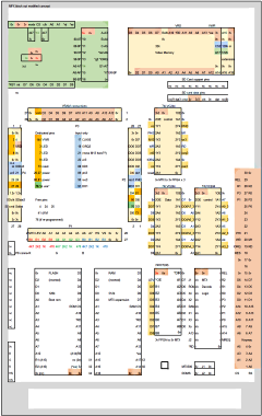
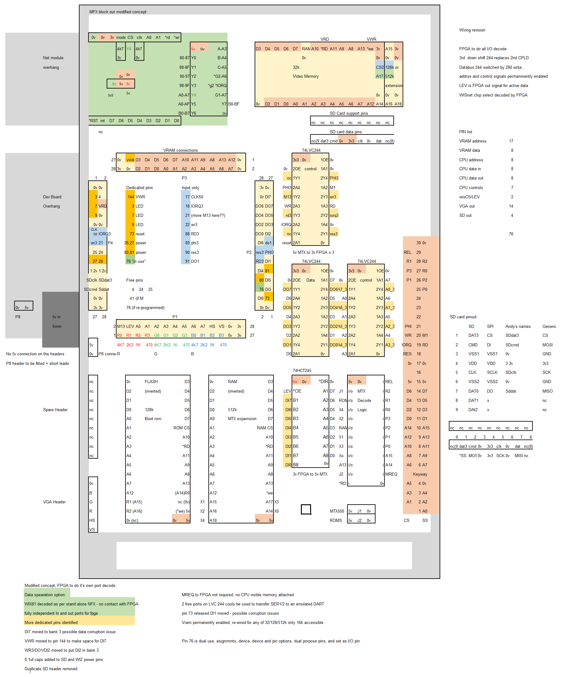
Likely
close to the final design, Martin's latest layout plan,
updated to include the extra capacitors and show the
data bit connection changes.
At this point, with
the design expected to be essentially complete, the FPGA
logic was only using around 38% of the available
resources and Martin's thoughts turned to how he might
utilise that spare capacity
Some potential
enhancements were :
add multi-colour mode and
G1.5 that Andy hadn’t implemented
add in
Andy’s math accelerator
add in some V9938/58
modes, e.g., Text 2 as used by
MTXplus
use the spare pins to have 2 VGA headers instead of one
switchable
use the spare pins for a simple
RS232 port
We discussed the pro's and con's of
the above and a few other ideas, but nothing was firmed
up at this stage. |
 |
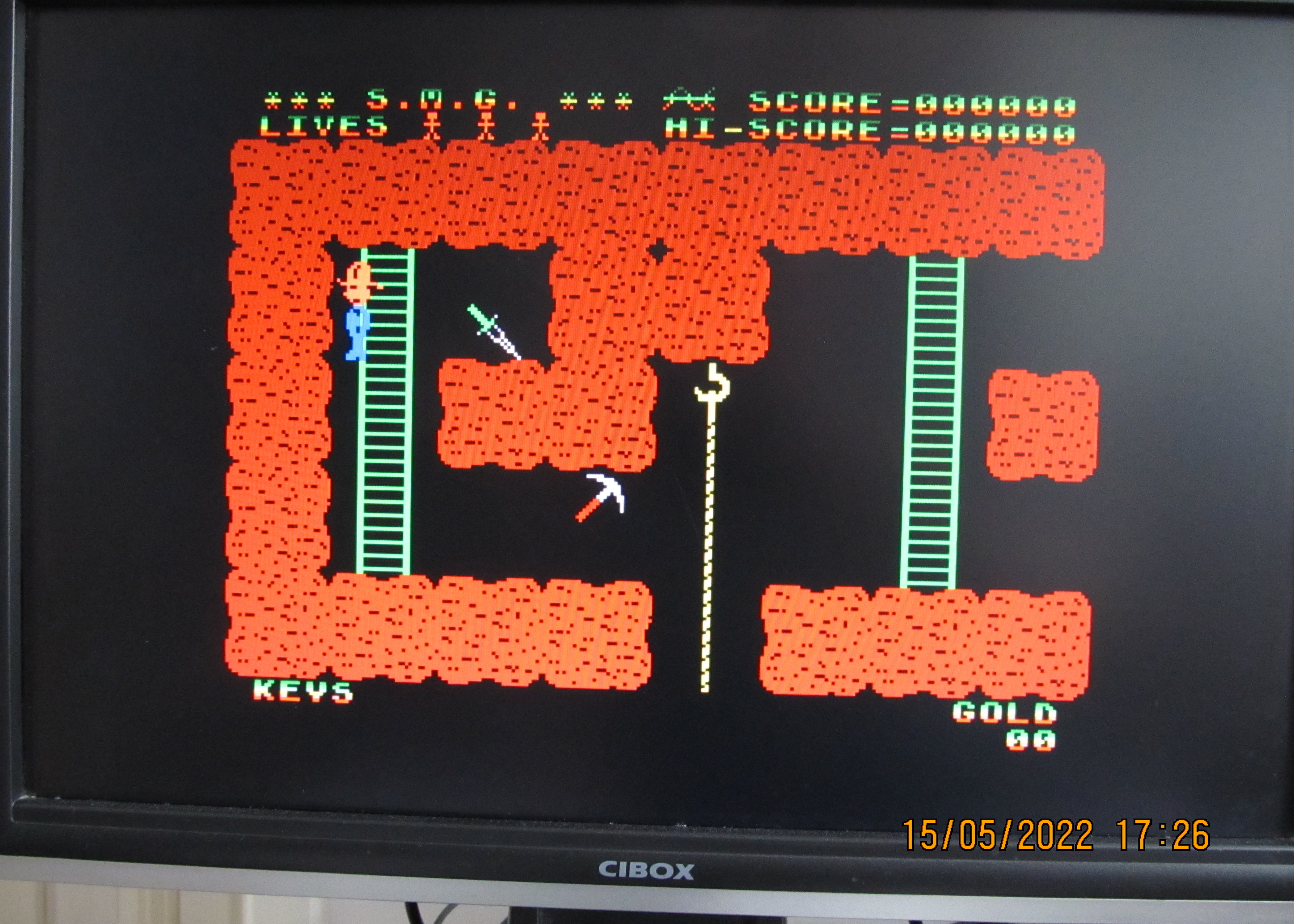
Additional
reboot tests went well, with nice clean start-up and
some CP/M side testing done in NewWord.
A few
other games were checked with good results, including
SMG shown here, which gave Martin some confidence that
there weren’t any major clock sync issues. |
 |
Oddly, Andy's Turbo
managed to break the sprite emulation - the car in the
street race level failed to update, so some
investigation and further work was required which turned
out to be quite straightorward.
It seemed that
Andy used G2 mode for the race track and G1 mode for the
street race. This highlighted the fact that the G1
sprite code had not been updated when Martin re-wrote
the code to reduce the sparkles. One cut and paste and a
re-compile later and Turbo was now updating sprites
correctly in the street race.
The next step
would be to take the CFX codebase, splice in Andy’s SD
card routines instead of CF and re-write the 80 column
bits to use the “new” display.
One idea that I
had for inclusion was to have some sort of SD card
activity indication. CFX, CFX-II and REMEMOrizer all
have easily visible LEDs to indicate CF/SD "disk"
activity. With all of the components of MFX intended to
be internal, this was not going to be an option, so I
suggested that some sort of on-screen indicator should
be included.
We also discussed the media that
would be required for the SD card slot. Andy's web pages
for REMEMOTECH and REMEMOrizer both suggests that the SD
card used should be no larger than 1GB. Cards as "small"
as this are becoming less common and we had some
concerns about their long term availability (potentially
a similar issue to the lack of availability of CF
cards). To better understand the 1GB "limit", Martin did
some research around SD/SDHC differences and found that
1 gig or smaller SD cards a guaranteed to
have a block size of 1 sector, 512 bytes
2 gig
SD cards report 1024 byte blocks, but should still
accept 512 bytes clock read and write commands
SDHC/SDXC cards use a different sizing system and uses
blocks between 4k and 64k
Trying to deblock a
card with 64k sectors would be very inefficient; to
update update one entry in the directory would mean
having to read and write 64k of data - SDHC support was
not going to be an option and this likely explains why
Andy stipulates cards of 1GB or less.
Since
Andy's SD/CF file system only supports 8 x 8MB
partitions (64MB), I had envisaged that a 64/128MB would
be adequate but Martin pointed out that 512MB would be
better as it would allow Andy's
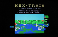
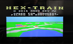
HEXTRAIN game to be loaded. This prompted Martin to
test its operation on MFX. |
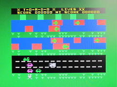
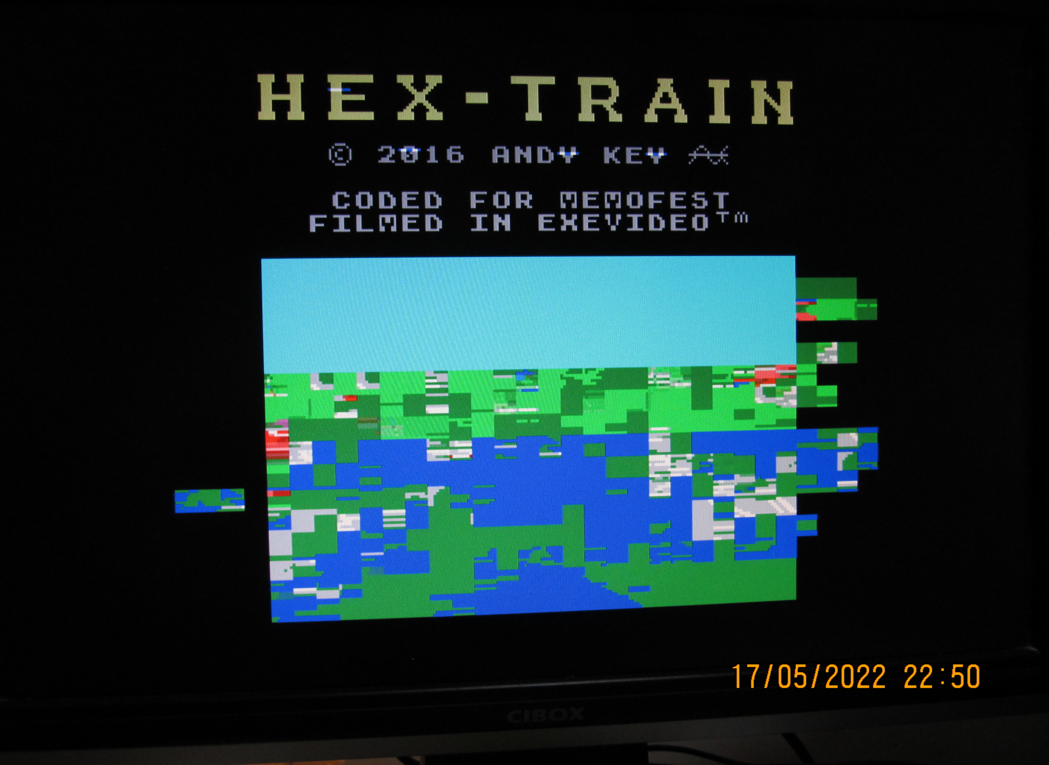
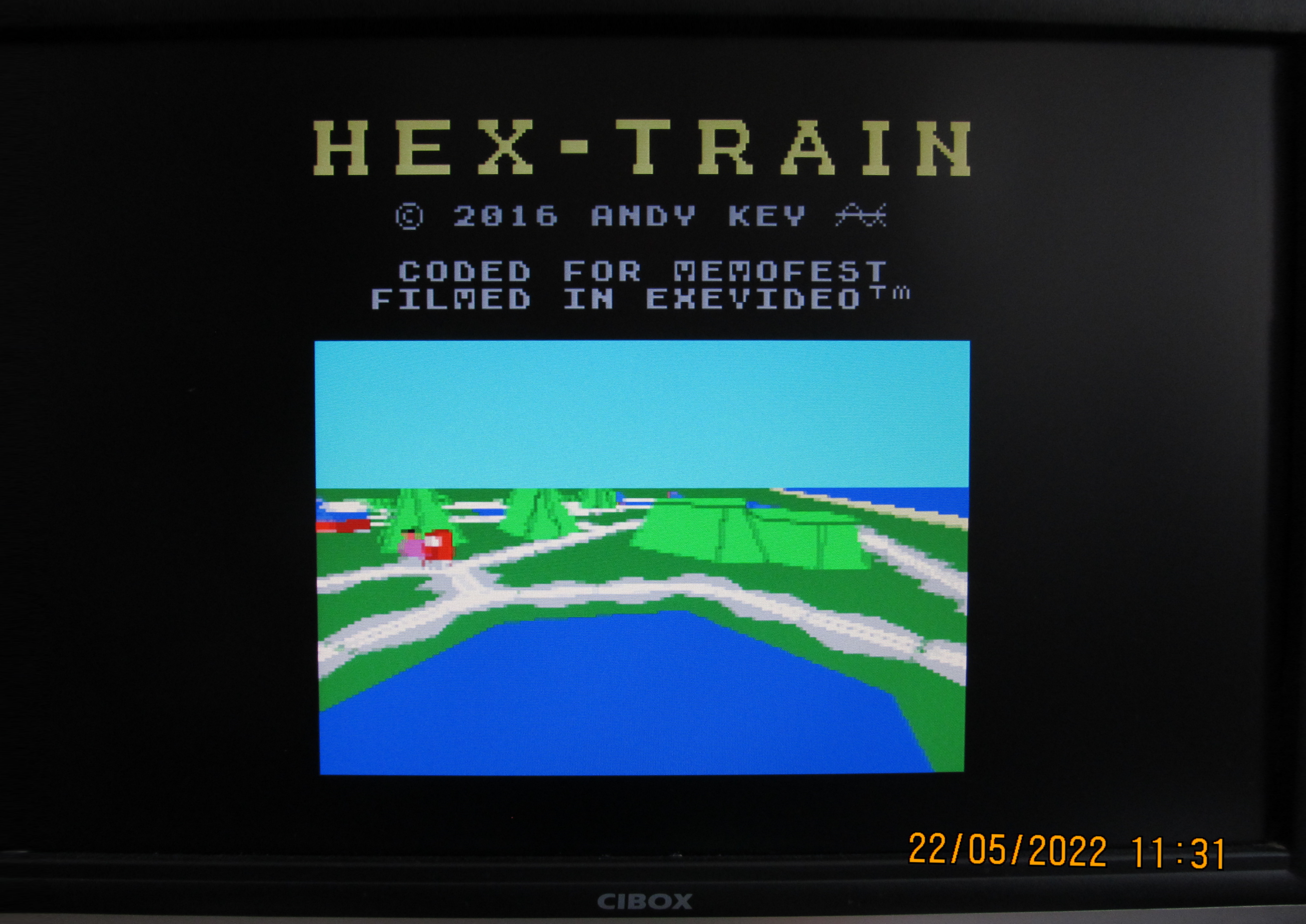
When
Martin first tried HEXTRAIN, the HTSD version from
REMEMOrizer loaded fine and the output from the VDP was
as expected. However, screen corruption was evident on
the FPGA VGA output.
This game really pushes the
MTX to the limit and relies on cramming lots of data for
the VDP into the vertical blanking period. To read the
details, see Andy's page on the technical details for
HEXTRAIN. |
 |
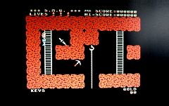
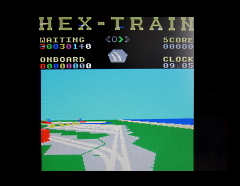
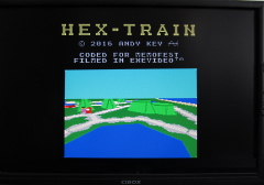
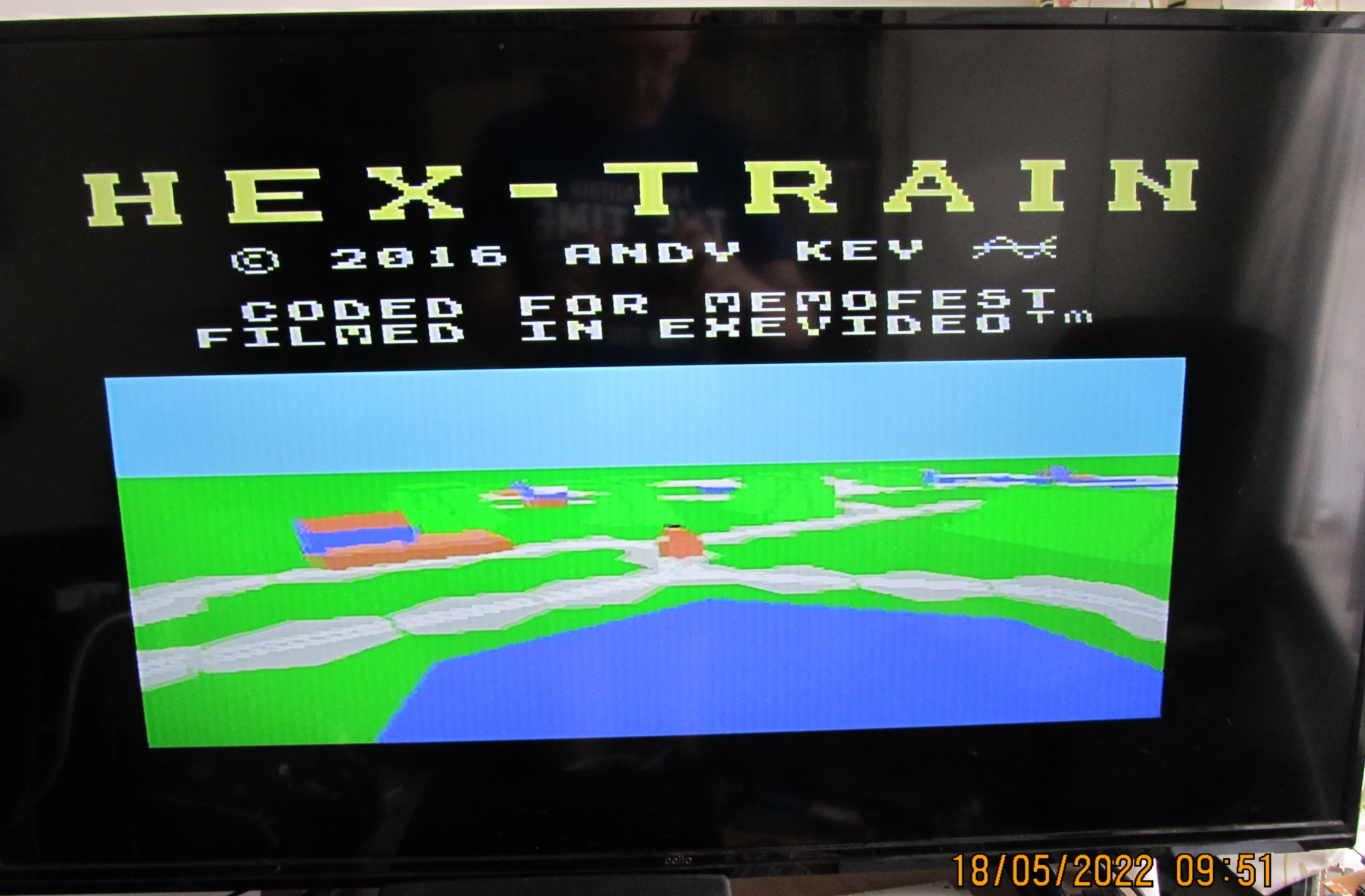
| For
comparison, HEXTRAIN's output from the MTX VDP. The
output was perfect, confirming the data was being read
from the SD card without issue. |
 |
Martin's
initial thoughts on HEXTRAIN were that it was an issue
with the shadow VDP implementation and very similar to
the problems that Andy saw when coding the
version for MTXPlus+, i.e., the problems were
possibly related to the CPU to VDP memory timings.
For HEXTRAIN, during the horizontal blank Andy
pushes pushes more data than when the VDP is drawing the
screen. Running on MFX, Martin felt that the problem was
almost certainly not the video generation itself, but
the corruption of what gets copied into the shadow VRAM
and noted that:
A: I
need my CPU to VDP memory access to work at the blanking
period rate all the time. There’s no way to synchronise
the 2 screens, even if the frame rates were the same,
and the default is they’re not!
B: The VHDL needs to be able
to cope with partial address updates. Which is one of
the tricks Andy mentioned on the MTXplus+ version write
up.
Some rough calculations suggested
that it was not actually a timing limitation; the shadow
VDP access slots for the CPU are 0.64us apart. A Z80
can’t generate requests faster than 2us apart, and even
allowing 3 CPU cycles for the time the I/O port is
active, there’s still 1.25us inactive, that’s double the
required amount. |
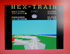
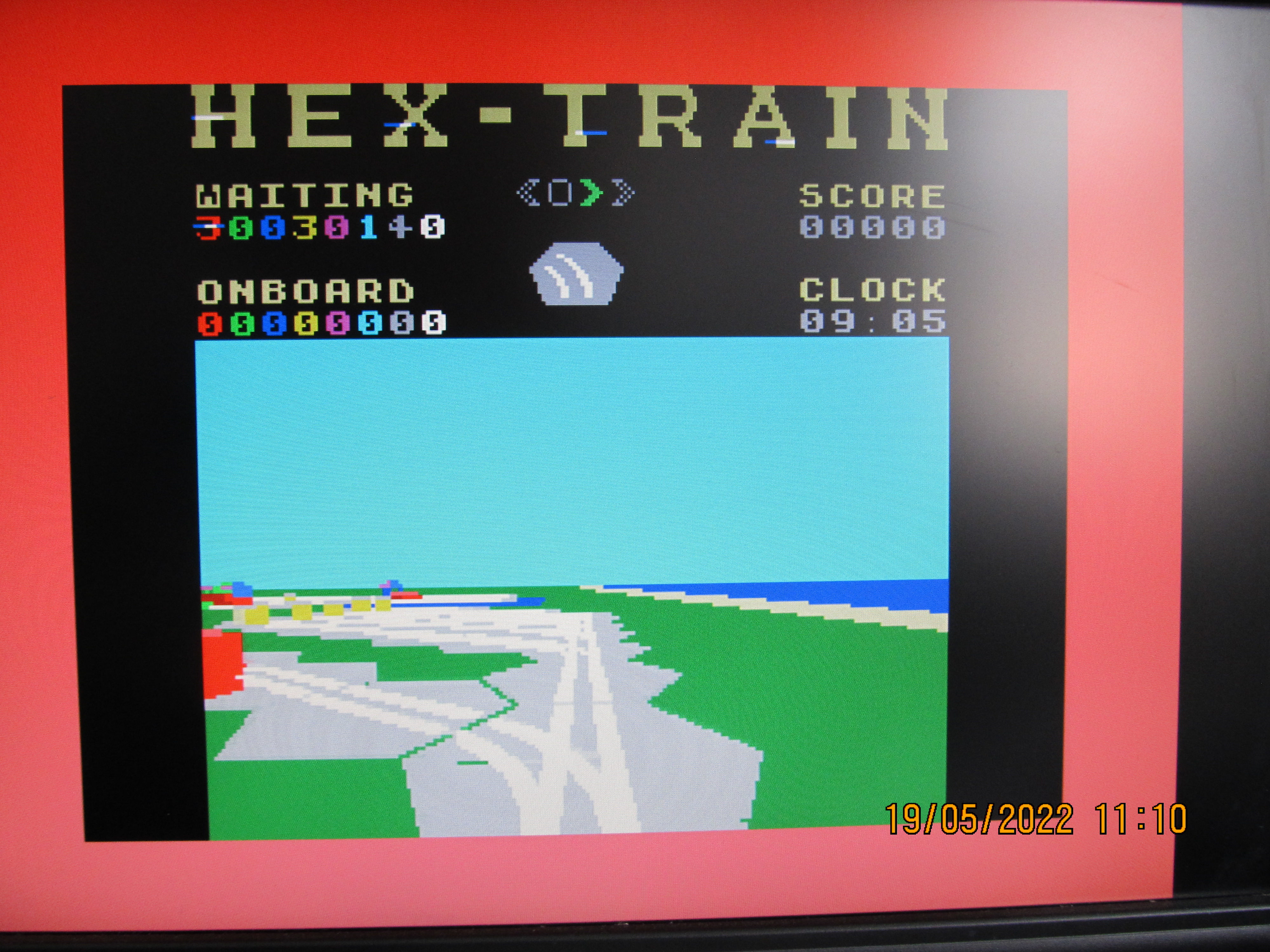
As noted
on
Andy's page, HEXTRAIN and a few other games only
output the low byte of the VDP address register if the
high byte is unchanged. Implementing this feature
eliminated the gross errors in the HEXTRAIN video
display.
There were still some minor glitches
that can be seen if you open the full size version of
this image. |
 |
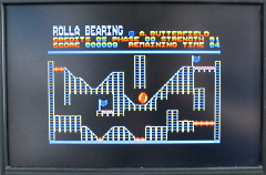
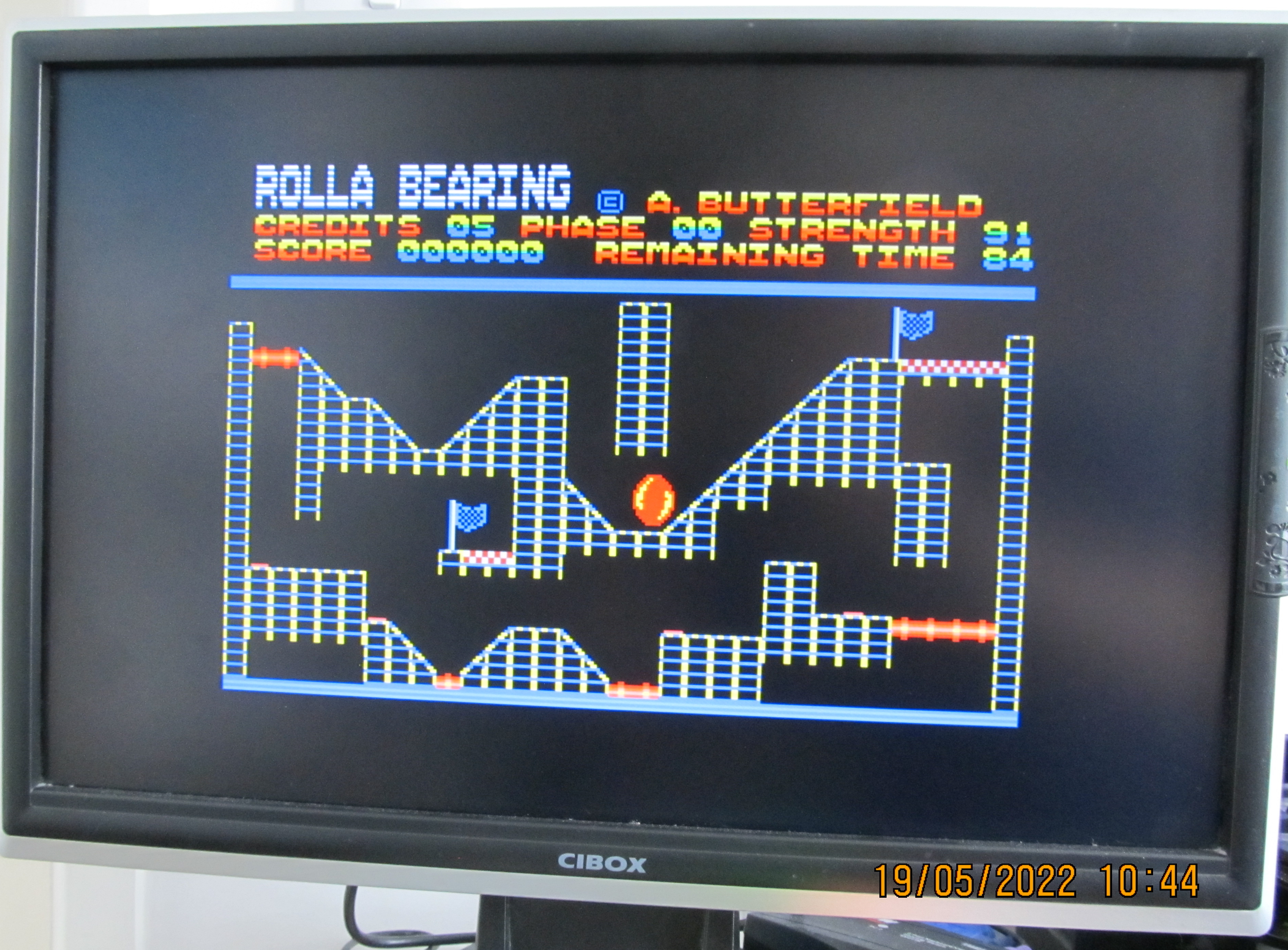
Martin had
also implemented an on screen disk activity indicator.
In 80 column mode, the cursor turns red when the disc is
active and for a short time after, just like a real disc
activity light.
In VDP mode, the border flashed
on the VGA screen. With "standard" MTX games, such as
Rolla Bearing, there was a brief border colour change as
the game loaded, then it reverted back to the defined
border colour once loading completed. |
 |
This
worked well, however, when used with HEXTRAIN, which
constantly accesses the SD card when the game is
running, it was distracting. The border “flash” flips
the top bit of the border colour when the SD card has
been accessed which is why HT is showing red (colour 1
flips with colour 9).
To prevent this, a “switch”
was added that enables the VDP border flash. The switch
is set by the SDX boot ROM, and cleared by the CPM boot
ROM. |
 |
When
implementing the "flash" feature, Martin found some
missing CPU to VDP transfer slots that were causing the
odd missed transfer.
Having corrected these,
HEXTRAIN issues now seemed to be resolved. |
 |
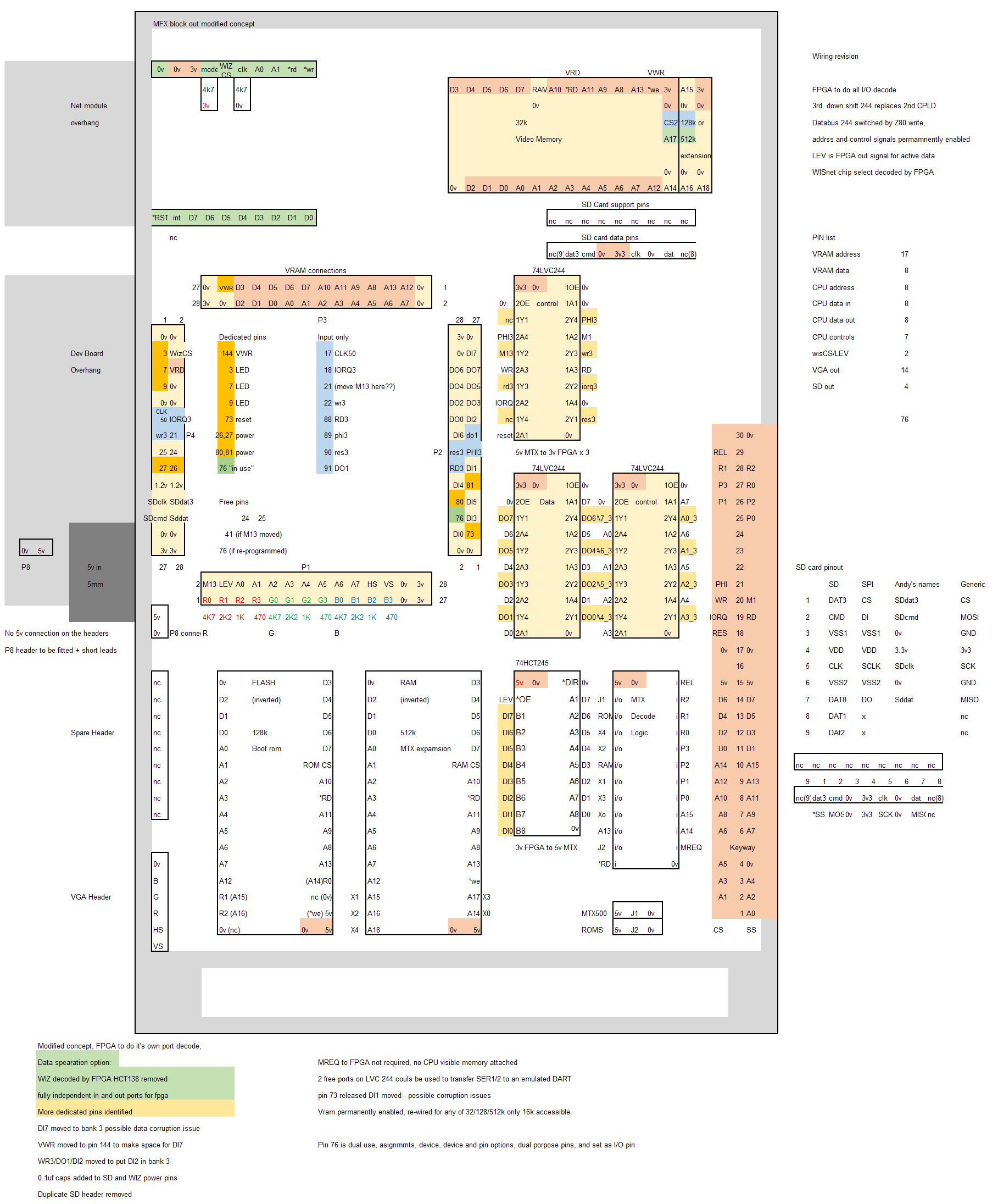
An
updated, perhaps final (?), update to the layout plan.
With plenty logic resources still available in the
FPGA, logic to decode the I/O address of the WIZnet
module was added to the FPGA. The 74HCT138 was no longer
required and could be removed.
A final word on
the (lack of) Speculator support in MFX. As noted
previously, whilst it would have been neat, it has not
been included, and is not possible for a couple of
reasons. Additional I/O decoding would be required,
which, in itself, would probably not have been too much
of a problem, but the main issue is the lack of
available I/O pins on the FPGA module. Both REMEMOTCH
and REMOMOrizer had level shifting capability on all of
the FPGA's I/O pins. With the FPGA board used in MFX,
level shifting has to be done externally and an
additional range of address lines (A9 to A15) would need
to have been made available to the FPGA to cater for
Speculator's Spectrum keyboard support. Unfortunately,
there were not enough spare I/O pins to allow this. |
 |
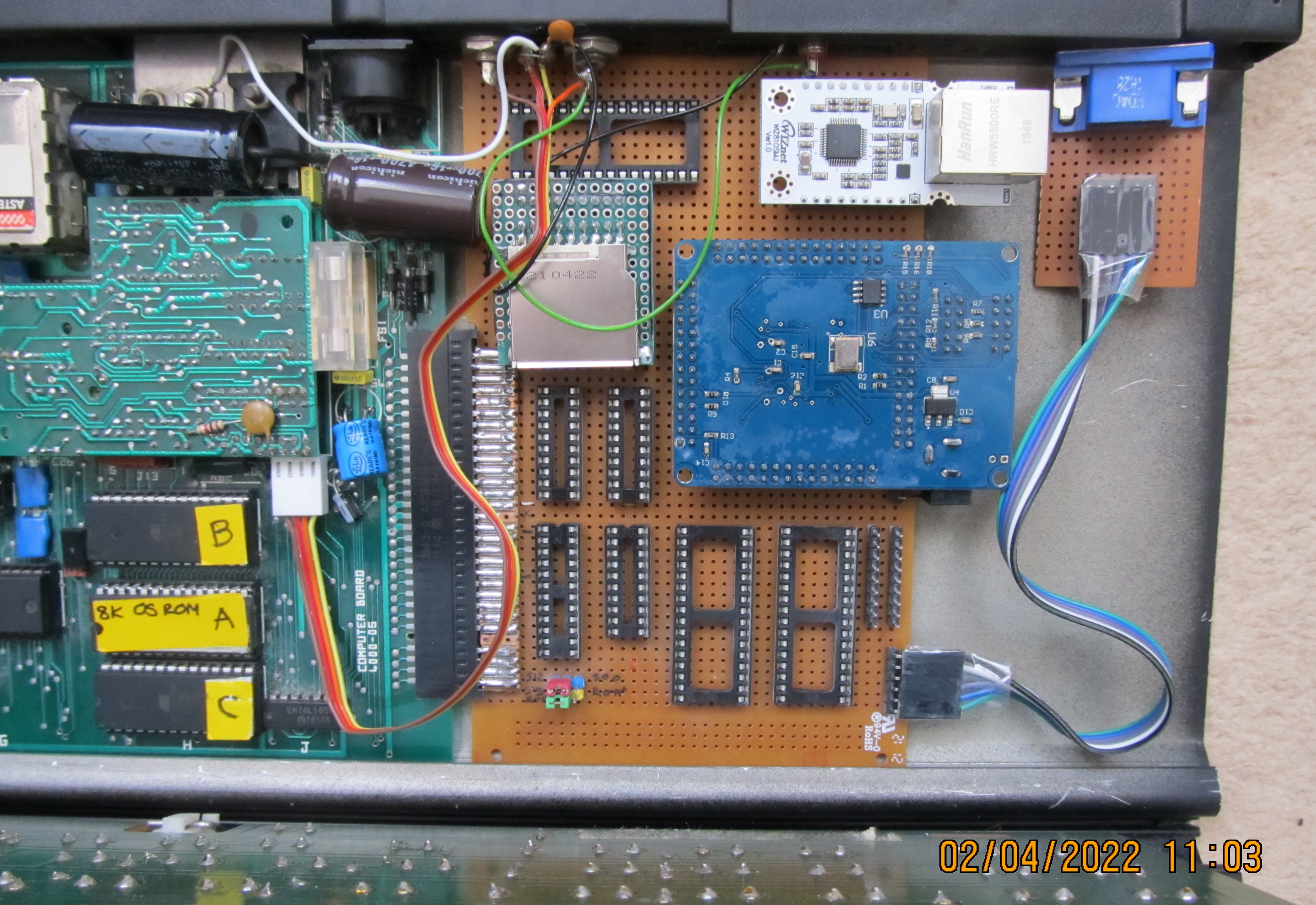
| During
development, Martin's FPGA board was powered from an
external DC PSU. When we checked how Martin's system
performed when the FPGA was powered from the MTX, a
small amount of "wobble" appeared on the VDP AV output.
Martin's MTX has a PS/2
keyboard interface fitted which most users wont
have, but provision
for an external 5VDC supply was added to the PCB design. |
 |
With the design
essentially complete and FPGA I/O allocation finalised,
it was time to take a closer look at the detail of a
suitable PCB design.
Over to Dave for that bit .
. . . details will be available
here in due course
In the meantime, Martin
continued to develop the MTX ROM software that would
interface with the FPGA.
The starting point for
the firmware used by all of our xFX expansions are Andy
Key's
SCPM and MTX
SDX
BASIC ROMs. Starting with CFX,
Martin modified the firmware to support the CFX hardware
and added a number of additional USER functions.
CFX-II added VGA output
and an 80 column option for CP/M and MTX BASIC.
Initial testing of MFX was done using Andy's REMEMOrizer
ROM to prove the concept, the next steps were to develop
custom firmware for MFX that integrated Martin's
previous firmware enhancements and introduced the
modifications required to support the MFX hardware as
well as enhancements possible with the upgraded
hardware. Some possibilities were:
Additional colours available in 80 column SDX BASIC mode
Possible introduction of some of the enhanced V9958
graphics modes developed for
MTXPlus+
All
of these possible enhancements were to be included with
the hardware design frozen.
|
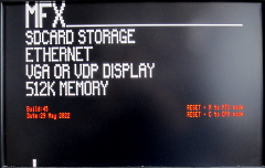
| VGA output
shadowing the VDP's 40 column text mode, displayed on a
wide screen monitor, set to preserve the 4:3 aspect
ratio. |
 |
| An early
version of the MFX specific boot ROM VDP output |
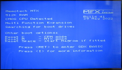 |
Corresponding Boot ROM output to VGA
Different
versions of the SDX boot screen were needed in CFX-II
due to the way that the Parallax Propeller VGA output
was configured. For MFX, the VGA output will default to
VDP shadow mode when booted into SDX mode, so separate
boot screens are not required and this screen never made
it into the final build. - Preserved here for posterity
! |
 |
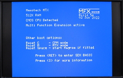
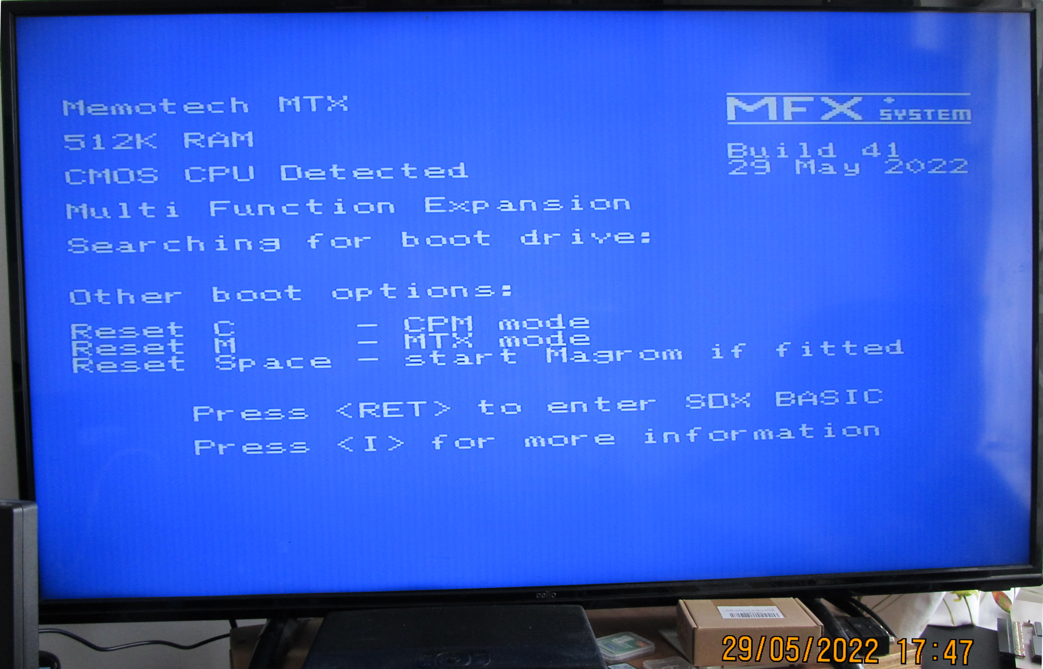
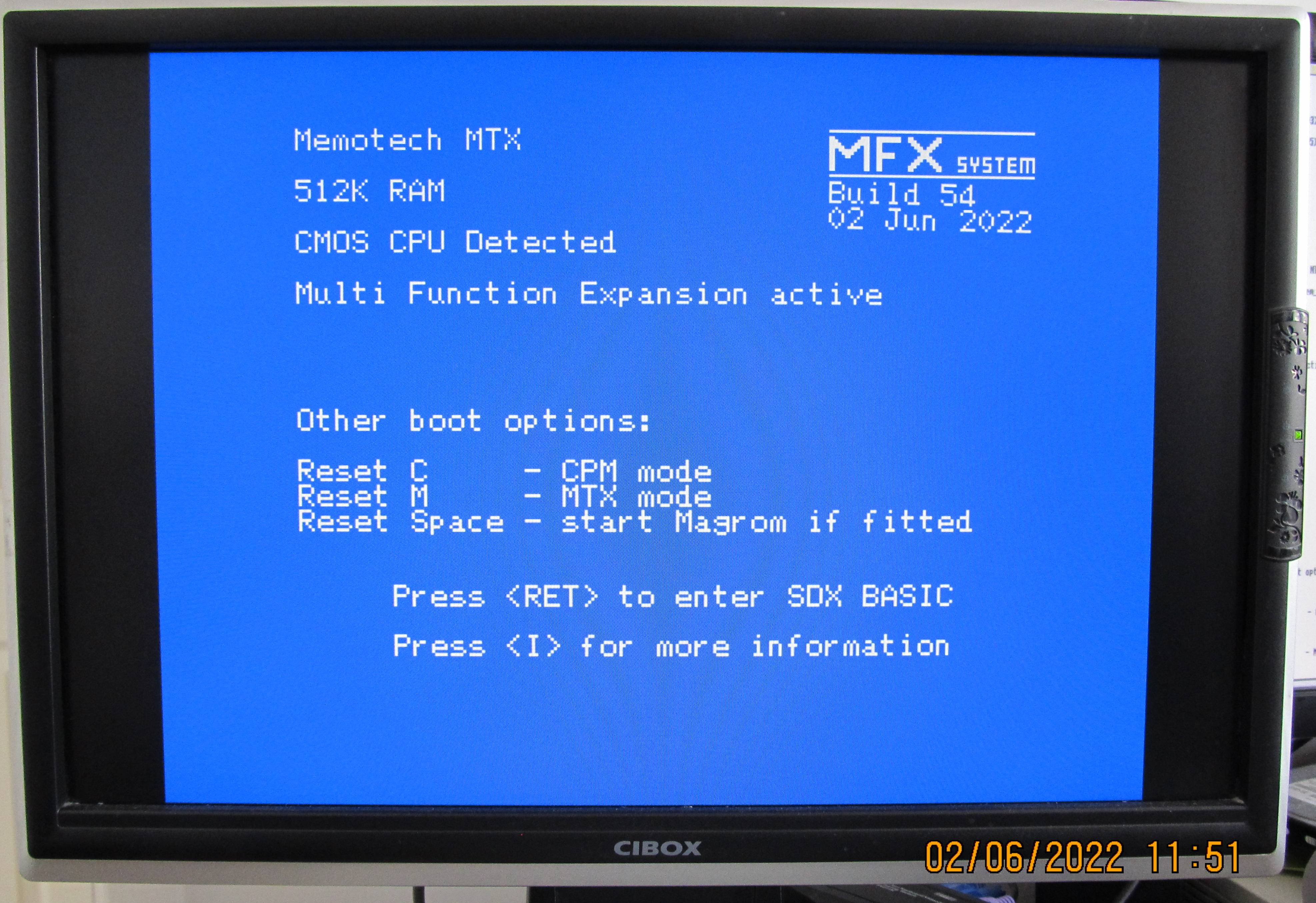
VGA shadow
of VDP output in SDX boot mode
In another change
from CFX, the "Searching for boot drive" string has been
removed. In CFX, the Compact Flash boot drive only gets
searched for on boot, in REMEMOrizer whose SD code has
been cloned for MFX , the card's presence is checked at
every access. |
 |
There have also
been some "behind the scenes" changes based on
suggestions by Bill Brendling and Andy Key
Readable Page Port Configuration
On the MTX computer, the Page port, (Output Port 0)
is used to configure ROM and RAM; paging memory greater
than the Z80's maximum address space of 64k in and out
of the 64k range as required. As it is output only, its
current state cannot be read back by the system. BASIC
keeps a copy of the page port in the PAGE system
variable, but CP/M has no way of knowing the current
page configuration. This makes it difficult for CP/M
drivers to make use of routines in ROM. Bill suggested
that a shadow copy of the page port could be stored in
the FPGA and another I/O address configured that could
be used to read it back.
Martin had already
created a control port for the FPGA. Since the emulated
6845 CRTC for the 80 column card uses ports 38h and
39h, like the original Memotech 80 column card, Martin
thought it logical to use 3Ah for the FPGA control port.
He has now created a readable page port at the next
address, i.e., 3Bh.
Screen Control
Optimisation
The BASIC clear to end of
line ROM function prints one space character the
required number of times to clear the text to the end of
the line. This takes approximately 100 Z80 cycles per
character. For the VGA output, it is possible to offload
much of the processing for this logic to the FPGA and
tell it to execute the character print code "x" number
of times. Executing the function using the FPGA means
that that each Z80 cycle can print 1 character - a
significant increase in speed in that particular
scenario on the 80 column BASIC screen.
WIZnet Port Assignment
Andy Key
maintains a
list of I/O ports used by Memotech and modern day
add-on devices. The NFX
prototypes used I/O ports A0 to A3 which are also used
by REMEMOrizer's arithmetic accelerator. After seeing
the NFX prototype, Andy suggested changing the I/O ports
used by NFX to unique port numbers. There are only a
very limited number of NFX prototypes in the wild, so
the impact in changing them for MFX is minor. However,
to support different port ranges, Bill has created new
versions of NFX.COM, FTPD.COM and HTTPD which have user
configurable I/O port address ranges. The port addresses
for WIZnet on MFX have now been changed to 90h to 93h.
A Minor Failure
As mentioned
above, one possible enhancement was the inclusion of
Andy's arithmetic accelerator into MFX. When Martin also
looked at this in detail, it turned out not to be
possible, Unfortunately, the code required over 5000
logic elements for the accelerator alone - with the FPGA
we're using only having a total of 4608 LE's, the
accelerator was obviously not going to be an option.
|
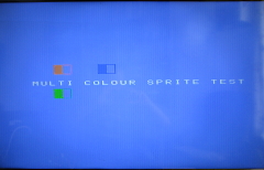
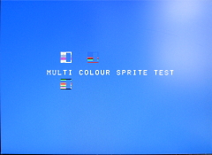
Enhancement - Multi colour sprites
The
TMS 9918 used in the MTX supports only single colour
sprites to a maximum of four on each scanline (although
a multi-colour sprite effect can be created by stacking
different colour sprites on top of each other).
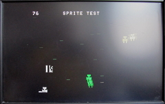
-
single colour sprites displayed by the MTX VDP |
 |
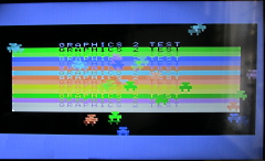
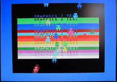
The
TMS9938 introduced multi-colour sprites and Martin has
implemented this as an option for the VDP shadow display
to the VGA monitor.
The colours are set on a per
sprite basis, so even if they use the same patterns as
in the screen shot, they can have different colours. It
makes it possible to do “MFX enhanced versions” of
games, without breaking them on the normal VDP display.
Martin has buildable sources for some games and may try
customising some games in due course. |
 |
Cloned
from CFX-II, Martin has
implemented an 80 column SDX BASIC text mode for
editing,
similar to that of CFX-II., but without graphics.
This is supported by the USER VGA command
|
USER VGA x |
VDP Output |
VGA Output |
| 0 |
40
Columns |
40
Columns |
| 1 |
(passive) |
80
Columns |
|
 |
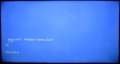
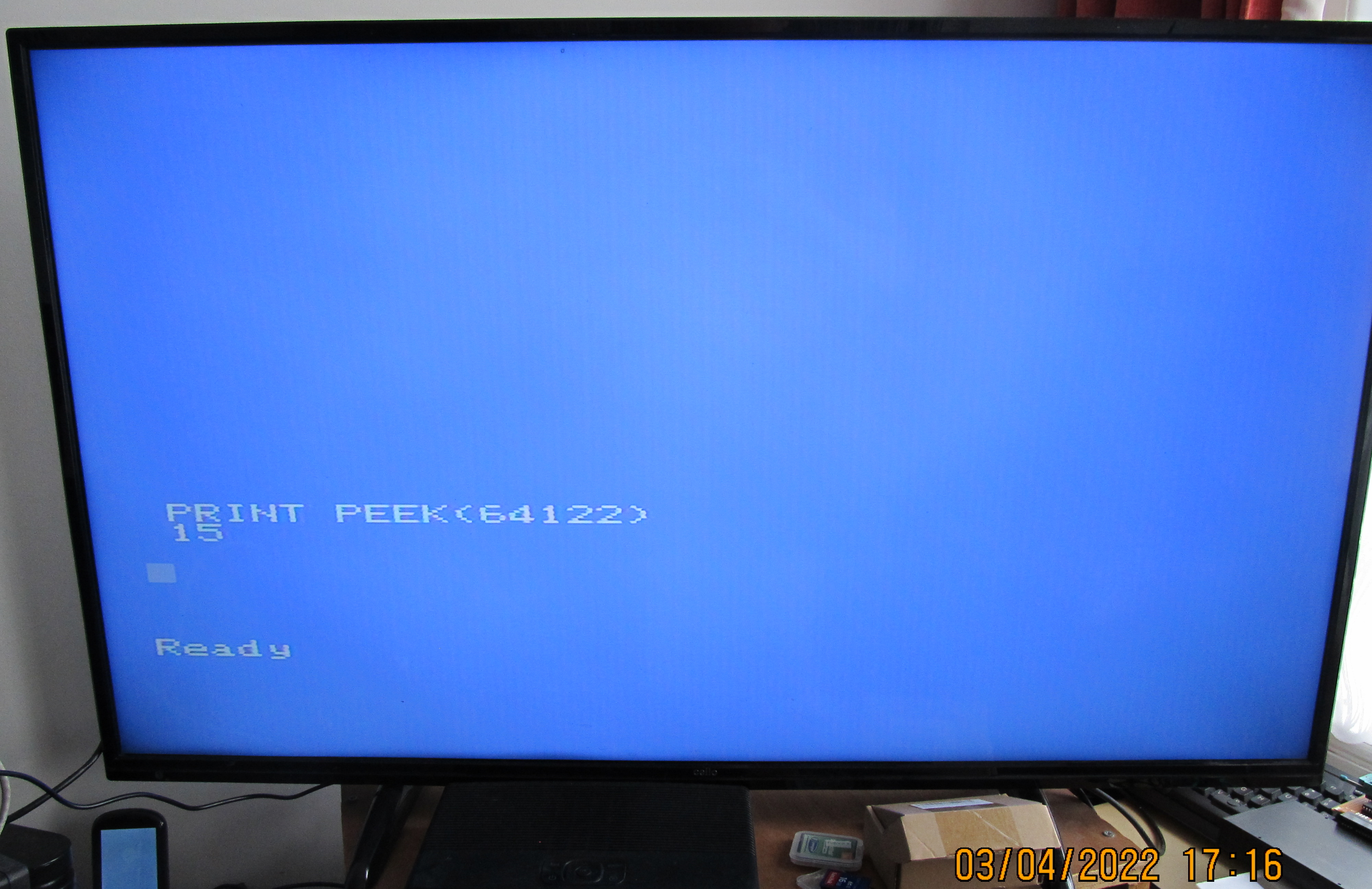
With the
FPGA having some unused RAM available, I suggested to
Martin that we should code a serial number into the FPGA
board.
Martin quickly confirmed that this was a
trivial task and implemented it, allocating 8 bytes of
read only storage, accessible via port 35h.
A
short from of the serial number will be presented on the
system boot screen - "MA00" in this example |
 |
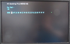
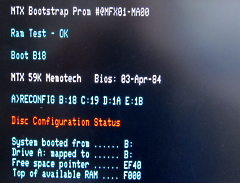
And also
displayed in the CP/M bootstrap PROM string
On
these screens, the serial number will display customer
initials and serial number.
Additional fields in
the serial number string will probably be used to record
the PCB hardware and firmware revision levels. |
 |
Other Video
Enhancements
The emulated VDP has a
choice of two colour paletts using either 3 or 4 bits
per pixel colour. The "rich" palette uses 3 bits per
pixel colour and the “historical” palette, more
representative of how the MTX video output looked on a
TV back in the day, uses all 4. Selection of the palette
is done by writing to I/O port 58d (3Ah)
|
In another
throw back to how the MTX VDP output looked back in the
day, Martin has implemented a vertical "hum" bar effect
in the VGA shadow mode, like you see on the MTX VDP
output.
(You will probably need to open the full
screen image to see them.) |
 |
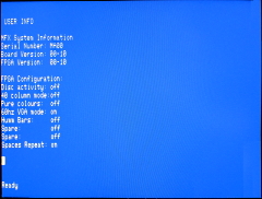
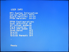
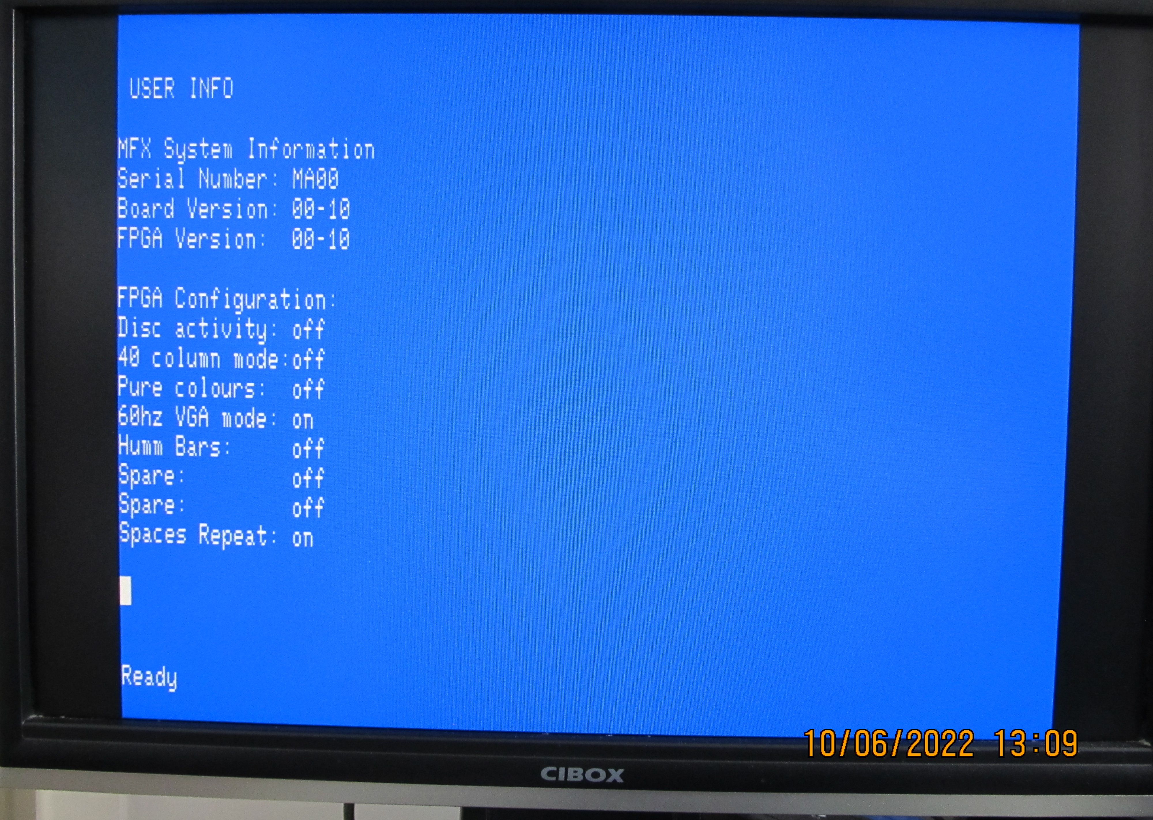
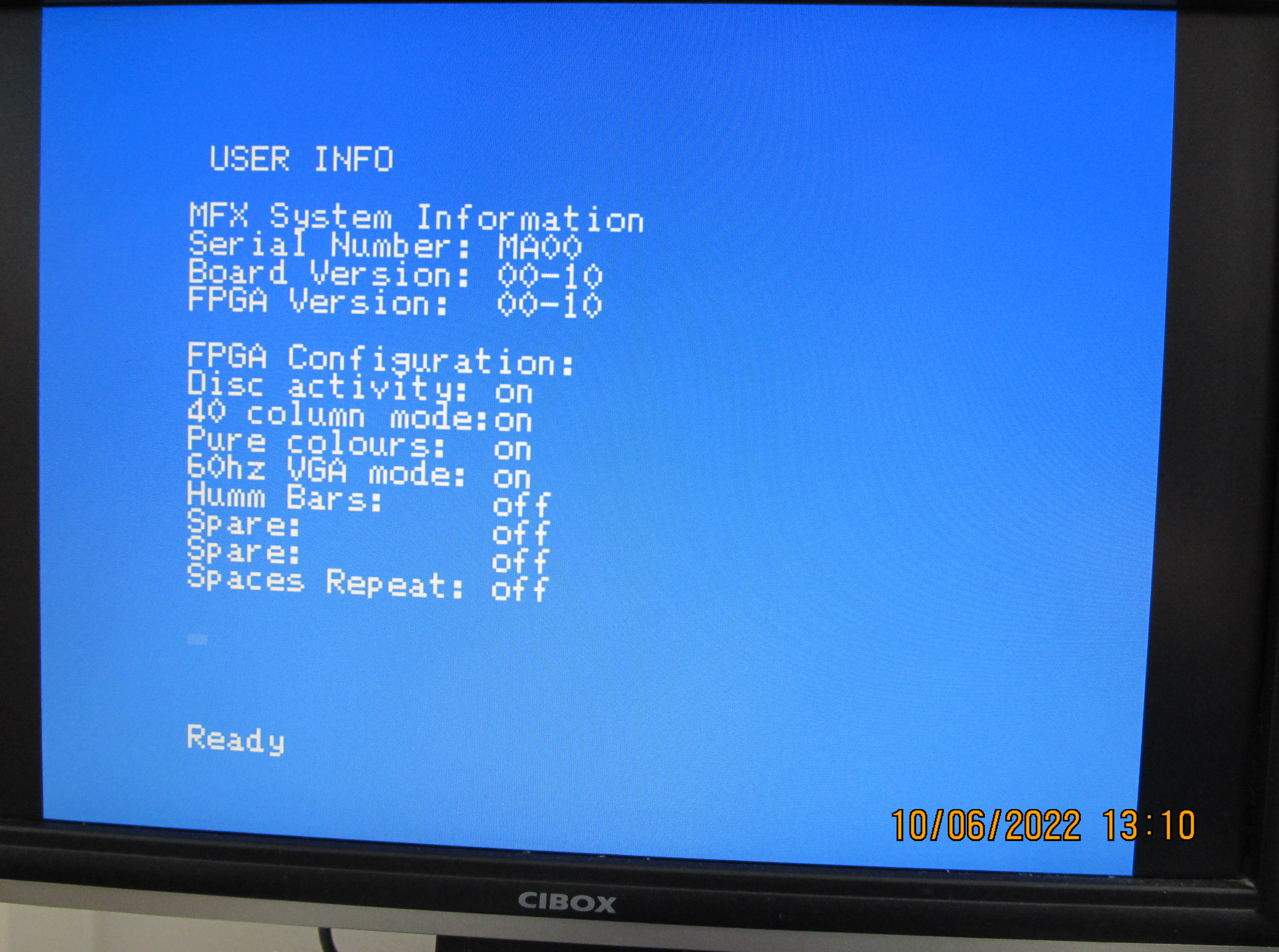
Now that
there were quite a few user configurable parameters for
the VGA output, Martin added a USER INFO option to the
SDX RM to provide a user friendly way to view these
parameters.
In 80 column mode . . . |
 |
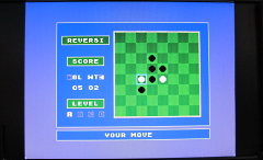
| And 40
column mode |
 |
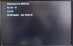
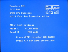
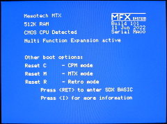
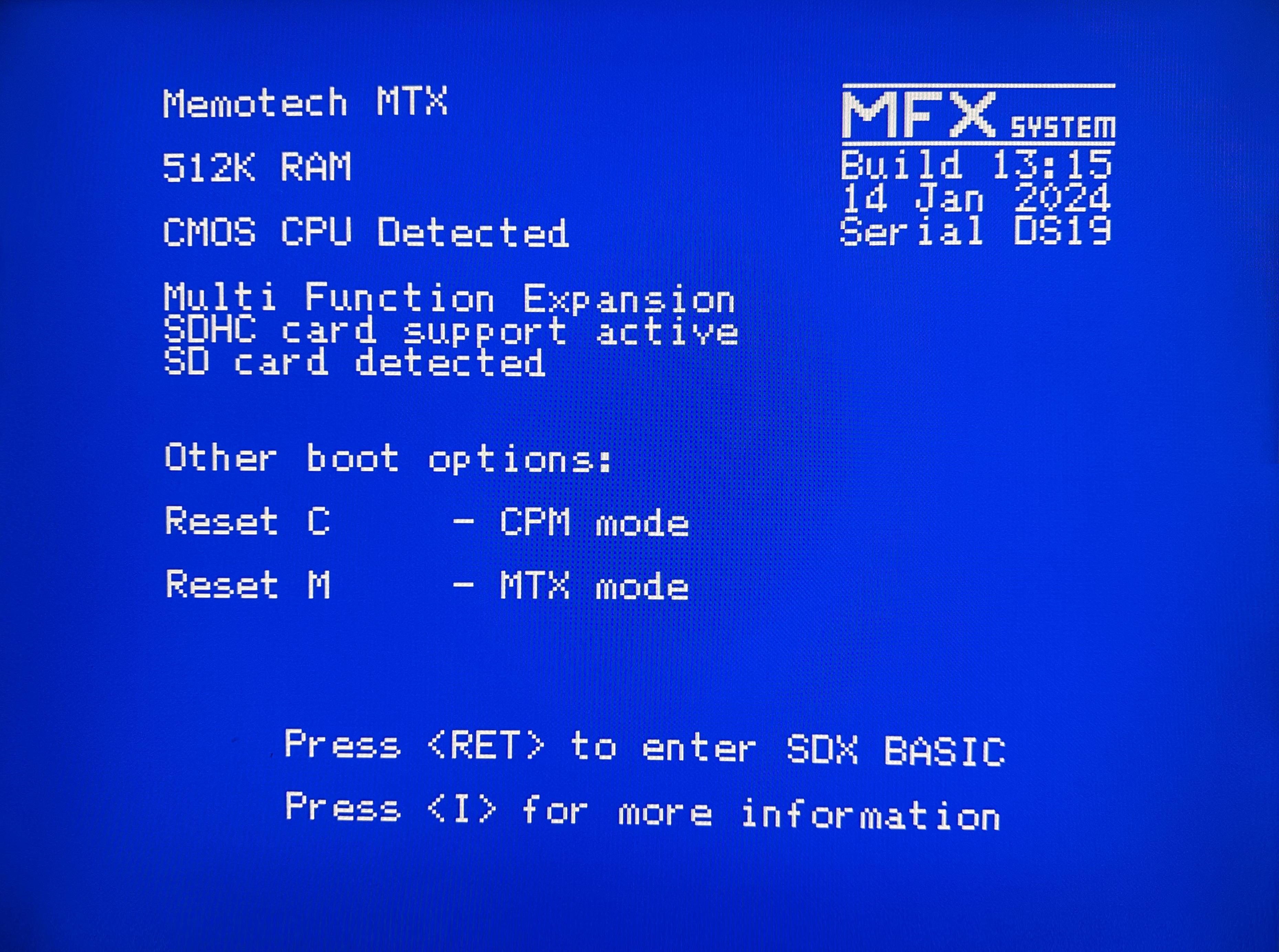
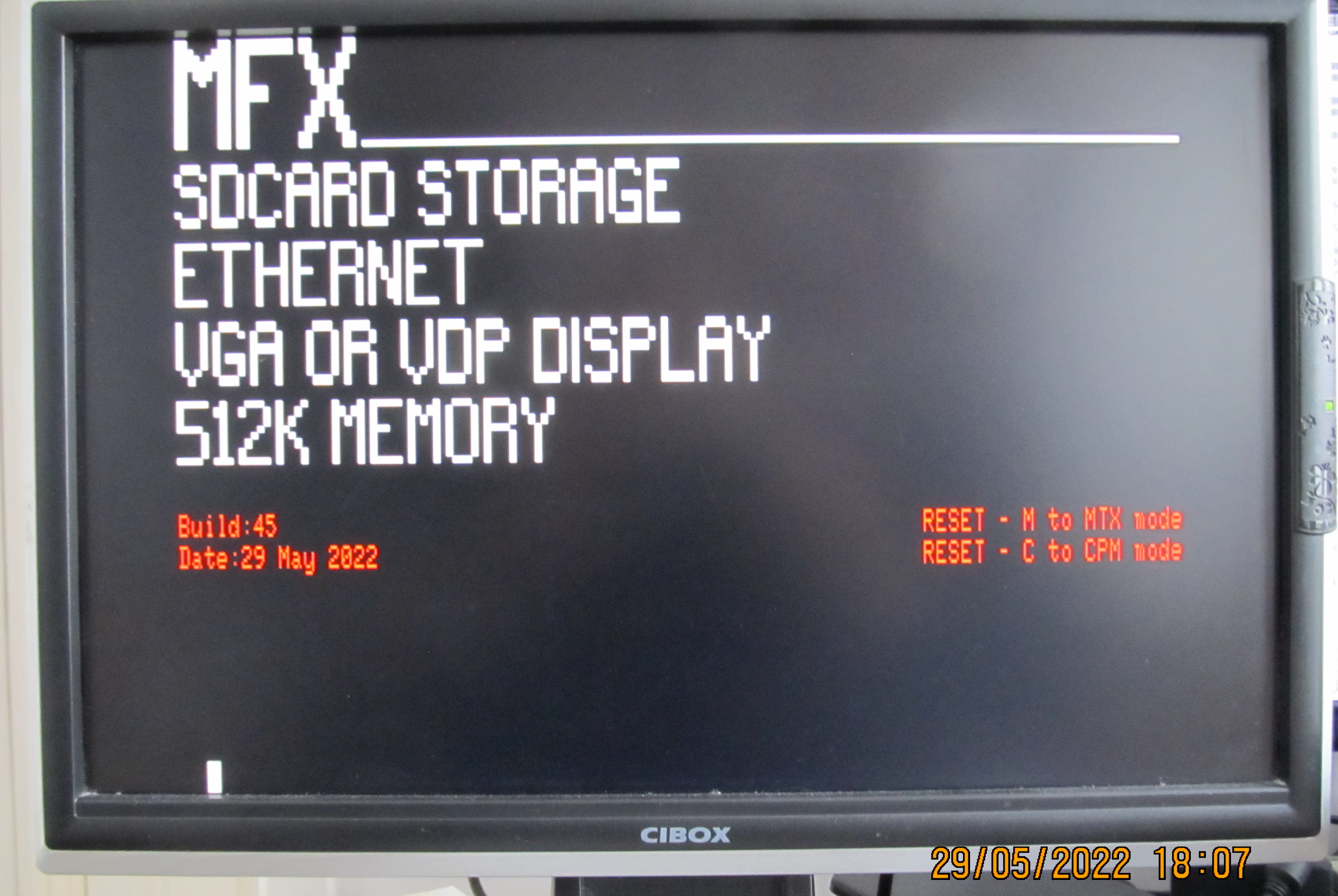
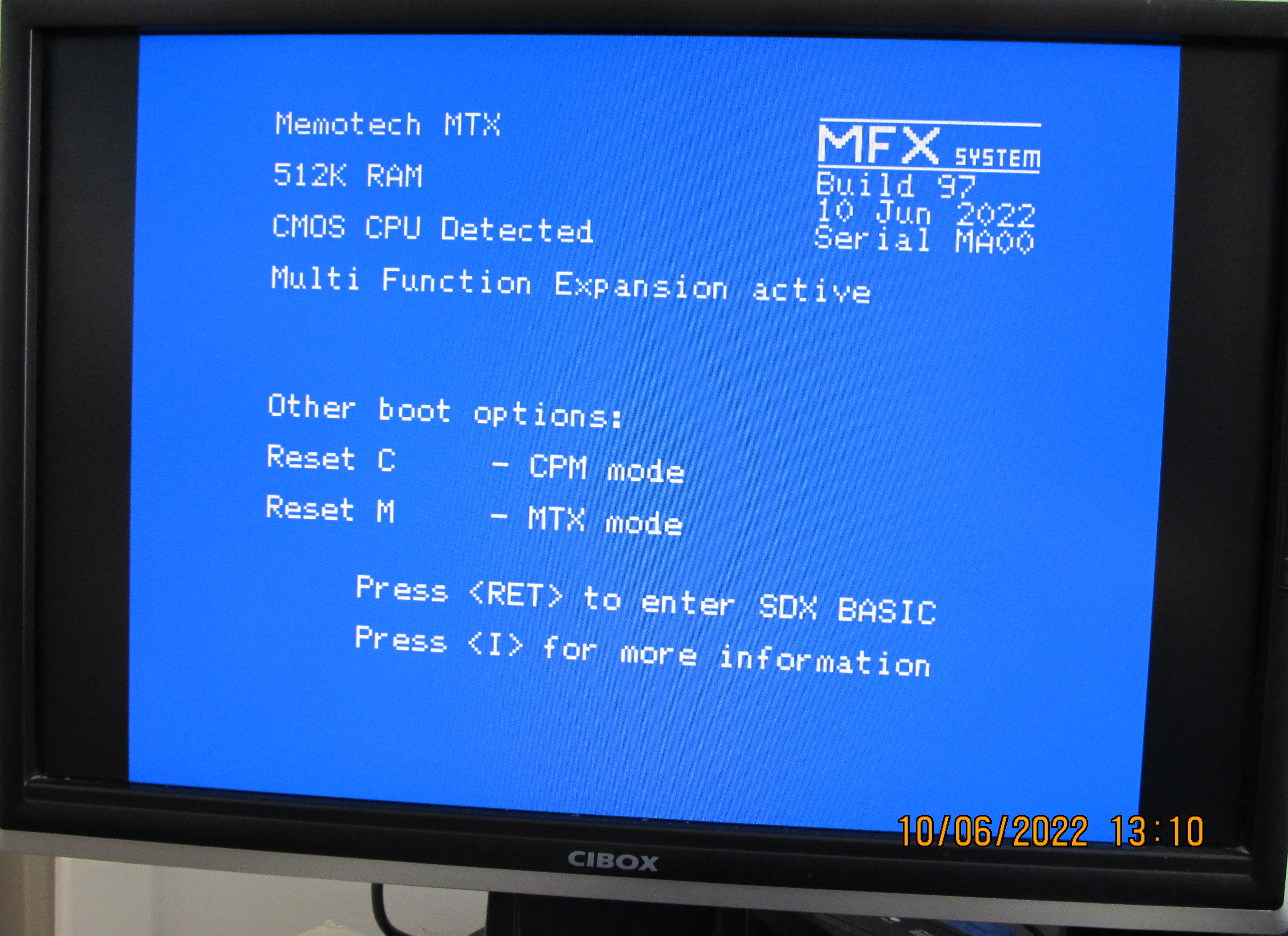
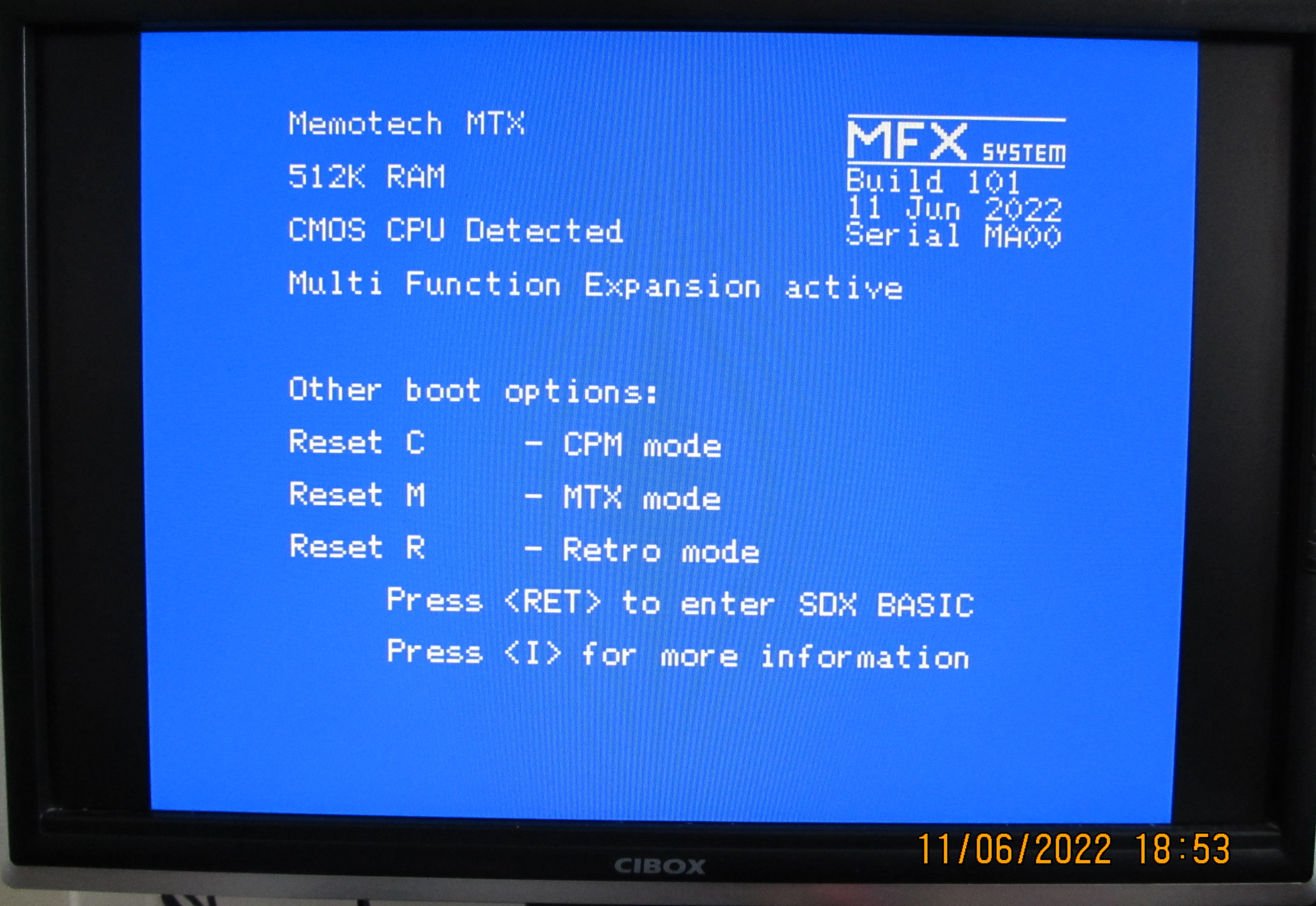
Final (?)
version of the MFX Boot Screen.
Although still
supported, the Reset <space> option to start
MAGROM has been
removed. The majority of games on MAGROM are available
as disk files, it is unlikely that (m)any users will
want to run MAGROM with MFX.
A new "Retro" mode
option has been created to invoke the vertical "hum"
bars and set the colours to the historical, less-vivid,
palette for a more authentic feel when playing games. |
 |
At this point,
the MFX firmware design was pretty much complete and our
focus moved to testing on the initial batch of PCBs that
I had manufactured.
Somewhat to my surprise,
despite the PCB design have no serious design or
manufacturing flaws, when running the firmware on the
PCB, a couple of issues came up. The problems and
resolutions are described in detail on the
MFX Engineering page. Suffice
to say, Martin was able to resolve these issues, updated
MFX PCBs have now been produced and finished products
are now being assembled.
|
| |
|


