|
 |
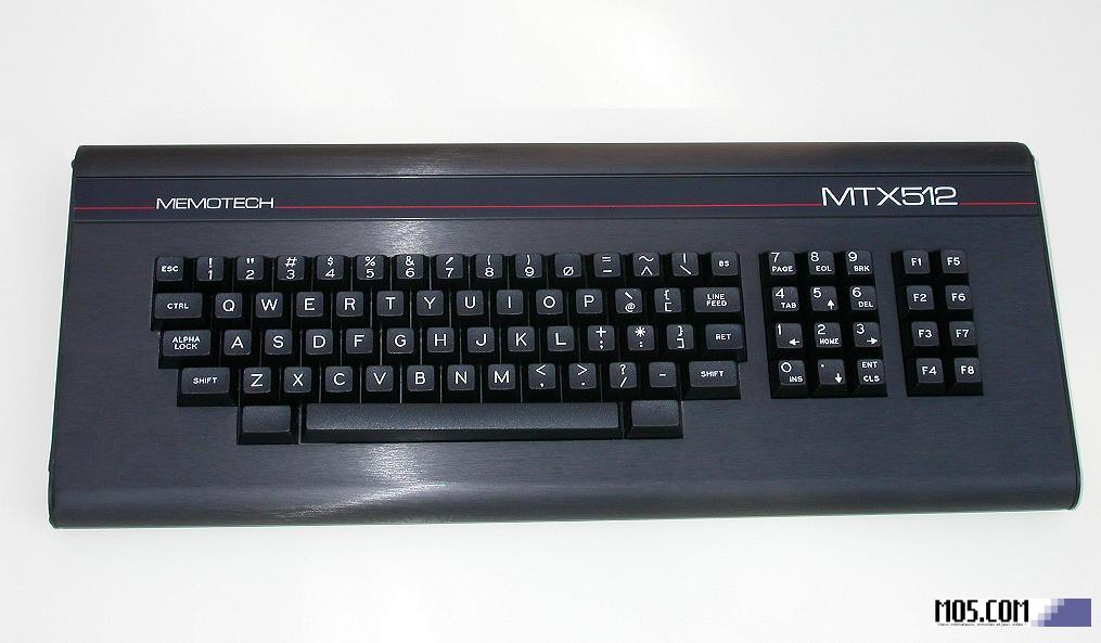
The Memotech MTX Series |
 |
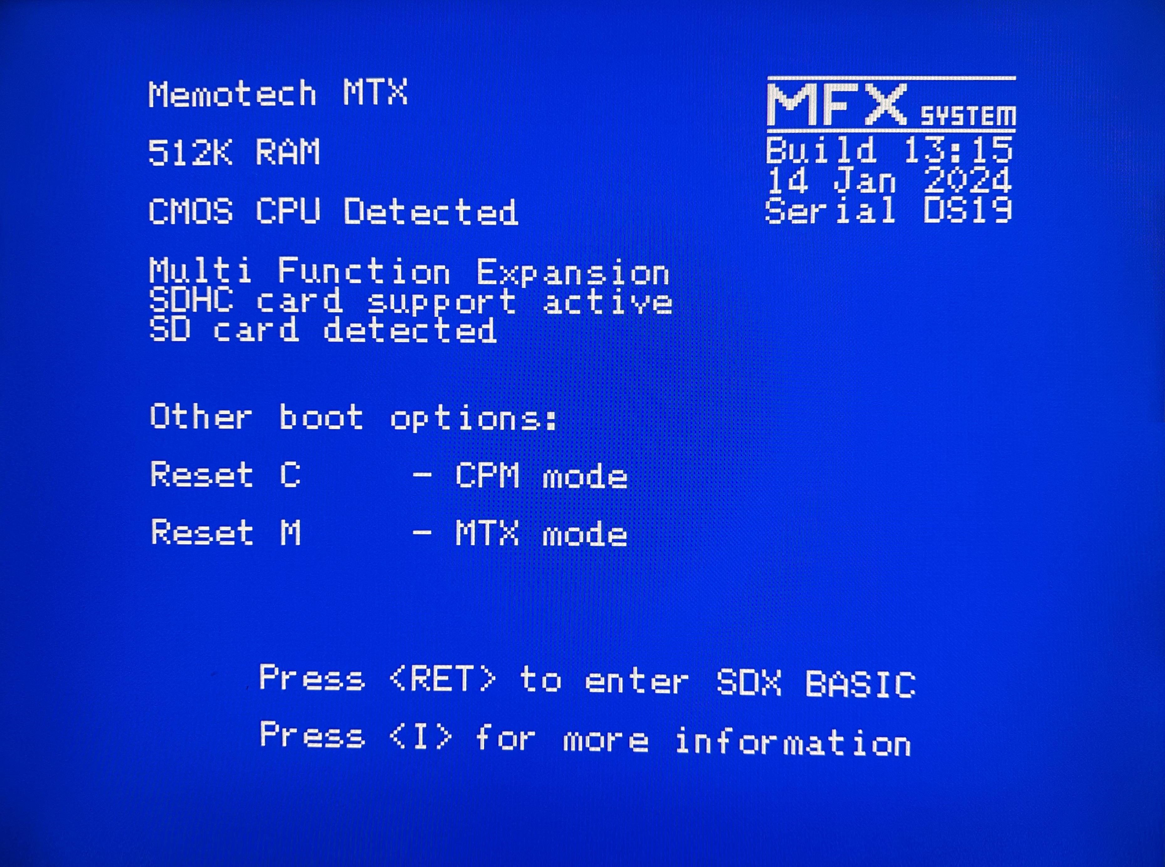
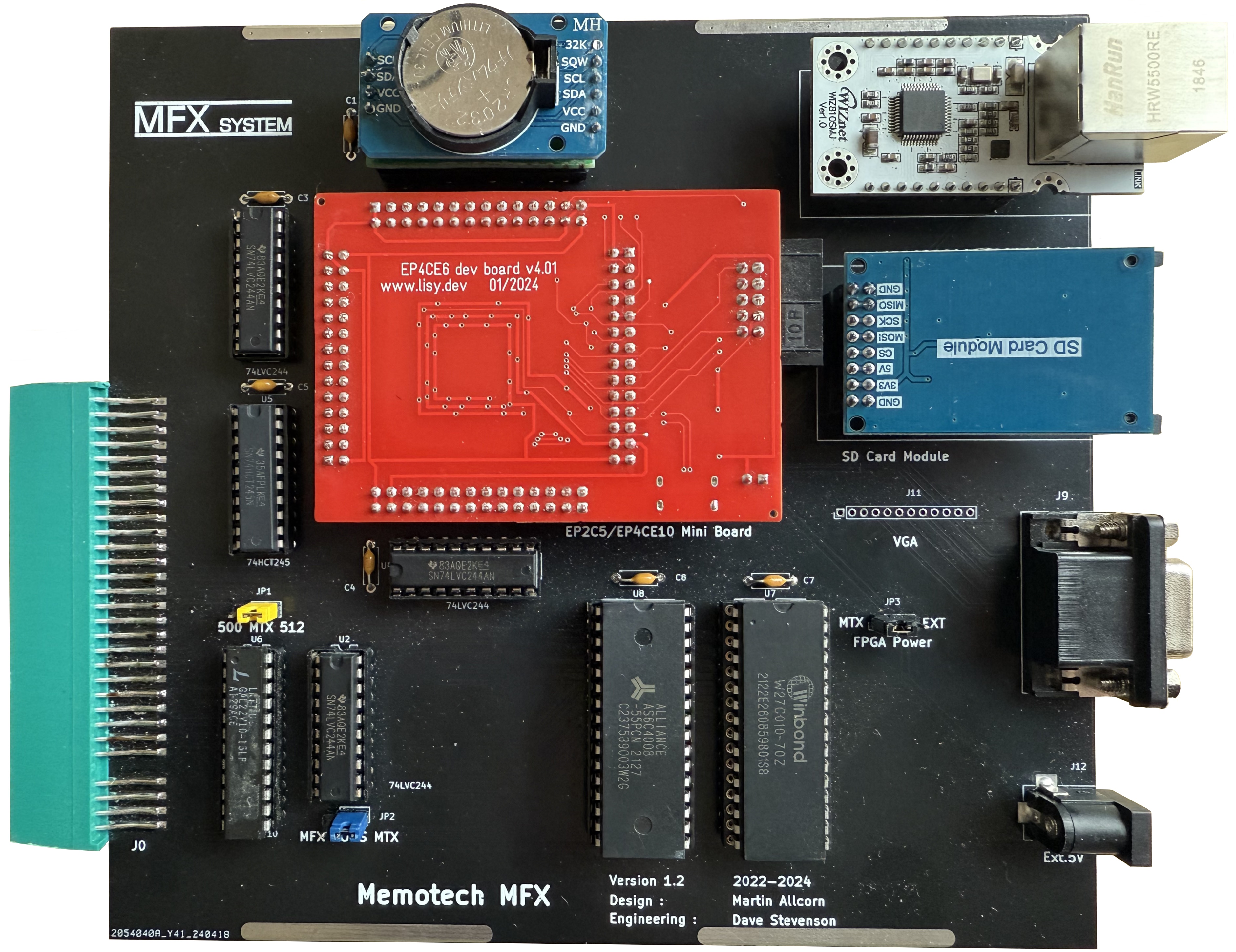
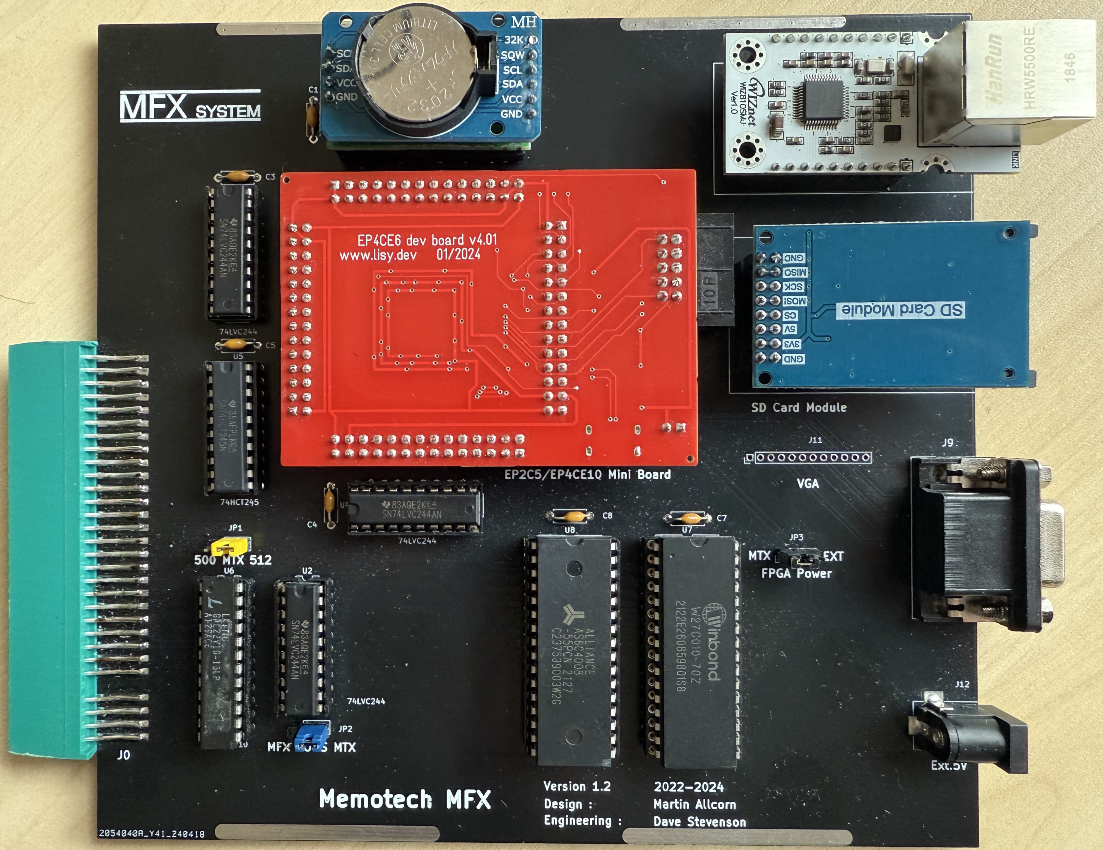
Memotech Multi-Function Expansion System
MFX Engineering Changes
one ?)
Engineering Changes
January 2024
This page describes the engineering
changes made subsequent to the first shipments of MFX. (The
firmware page describes minor
enhancements to the firmware, the focus on this page is purely
hardware.)
The biggest issue that I experienced when
completing MFX boards was
supply shortages and the variable quality of the FPGA modules
that we used in the design. (in hindsight, it would have been
better to use a device that was not so near the end of its
production life, but hey-ho!).
When MFX was released, the world was
still in the grip of the Covid pandemic and electronic parts
that were previously cheap and in plentiful supply suddenly
became scarce and correspondingly more expensive. It was hoped
that as the global situation improved, things would return to
something more like normality, but, even by early 2024, that
hadn't happened. The FPGA modules had increased significantly in
price, and although many Chinese sellers were advertising as
having them in stock, when orders were placed, they frequently
failed to deliver, and when they did, the quality was variable,
with many having faulty I/O, most likely due to poor quality
assembly, or possibly the use of factory reject FPGA chips.
Something needed to be done if MFX was going to continue without
a major redesign . . . . .
The FPGA module was so common and
(supposedly) available from so many different suppliers that I
thought that it must have been an Open Source project, at least,
originally, and as such, I expected to be able to locate the
original design files with a view to having them manufactured
and assembled by my usual PCB supplier. Unfortunately, I was not
able to find the design for the original board anywhere on the
web, however, I did find a possible solution . . . .
Ralf Thelen, the designer of a number of hardware projects
for legacy
pinball machines, had used the same FPGA development board
for a number of his projects and had experienced the same
quality issues that I had. As he notes on his website, "Because
of this I made a 99% copy of the [Cyclone II Development] board
which can be fully assembled by
JLCPCB." Ralf described this and included links to his
repository containing the design files
on this page
of his website, lisy.dev.
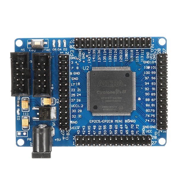
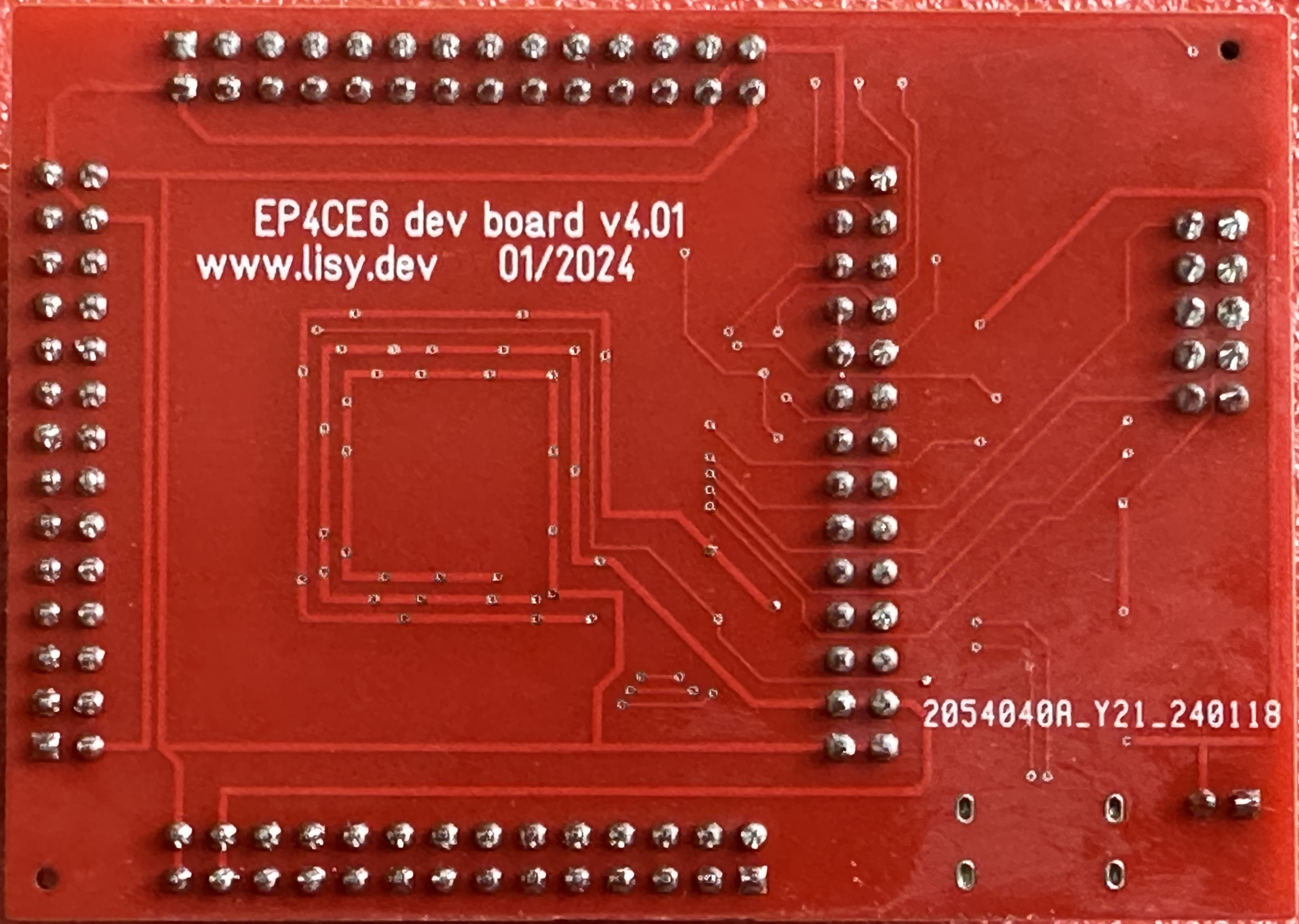
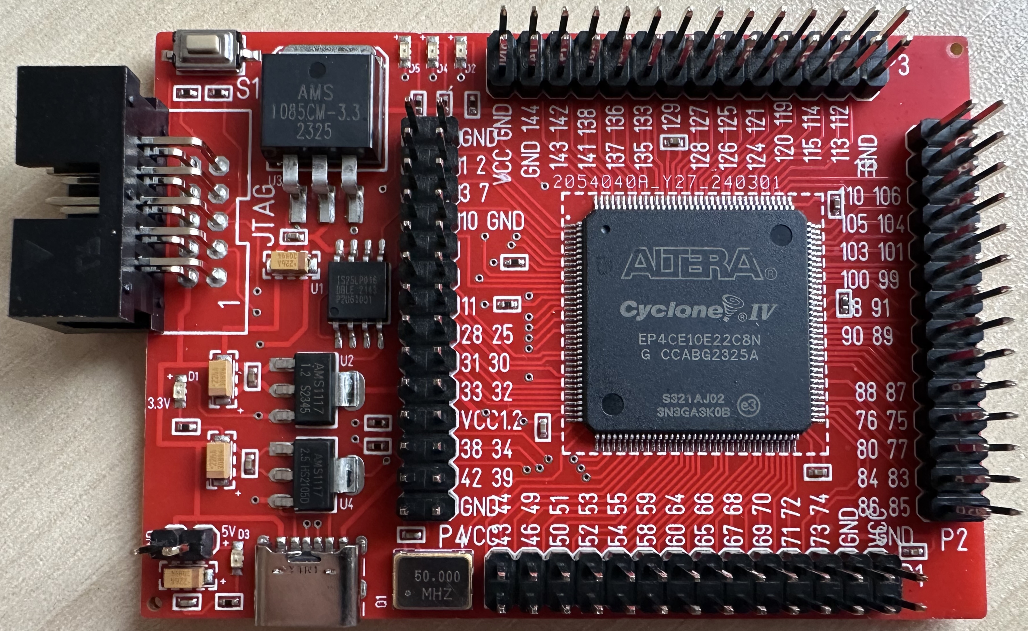
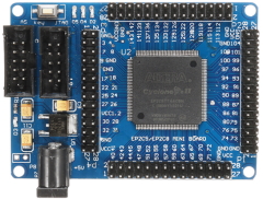
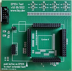
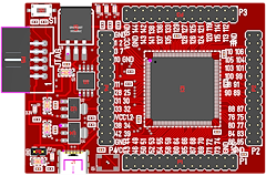
| The
original development board on the left and Ralf's on the
right - good isn't it! |
 |
 |
The most obvious difference is that the
JTAG port is
not fitted, but MFX doesn't need it - programming is done using
the
ASP port on the left. This made space to place all of the
components, including the oscillator and EPROM chip, on the
front side of the board which makes the cost of assembly
cheaper.
Obviously, this sounded like exactly what
I was looking for, but things got even better! Whist supplies of
the FPGA seem to be still available, at least in China, the
Cyclone II is obsolete and will surely become harder to source
before too much longer. I was really pleased when I saw that
Ralf had also done a version of the development board with the
same form factor for the Cyclone IV FPGA. This chip too is close
to "end of life", but should be available for longer than the
Cyclone II, with the added advantages that it is more powerful,
with additional internal memory and it is actually cheaper than
the Cyclone II.
It seemed that the Cyclone II version
would allow me to secure my own supply of development boards as
a like-for-like replacement for the originals and the Cyclone IV
version would also be a "drop-in" replacement with the added
benefit that the additional resources might offer scope for
further developments for MFX.
Having made contact with Ralf, I have to
say how helpful and supportive he has been. At this point,
things are at an early stage, but I am actively pursuing this
option . . .
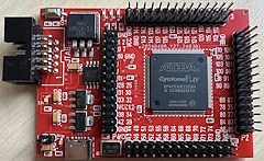
Ralf's
first Cyclone IV boards were for chips with a
BGA package. BGA provides access to more pins than
the
TQFP package so the development board, would in
theory, have more I/O capability, but as this is
constrained by the header configuration, the point is
moot.
JLCPCB charge more for mounting BGA devices
than TQFP, so Ralf changed his design to use TQFP
instead. Also note that Ralf has used a USB-C socket for
the external power connection. |
 |
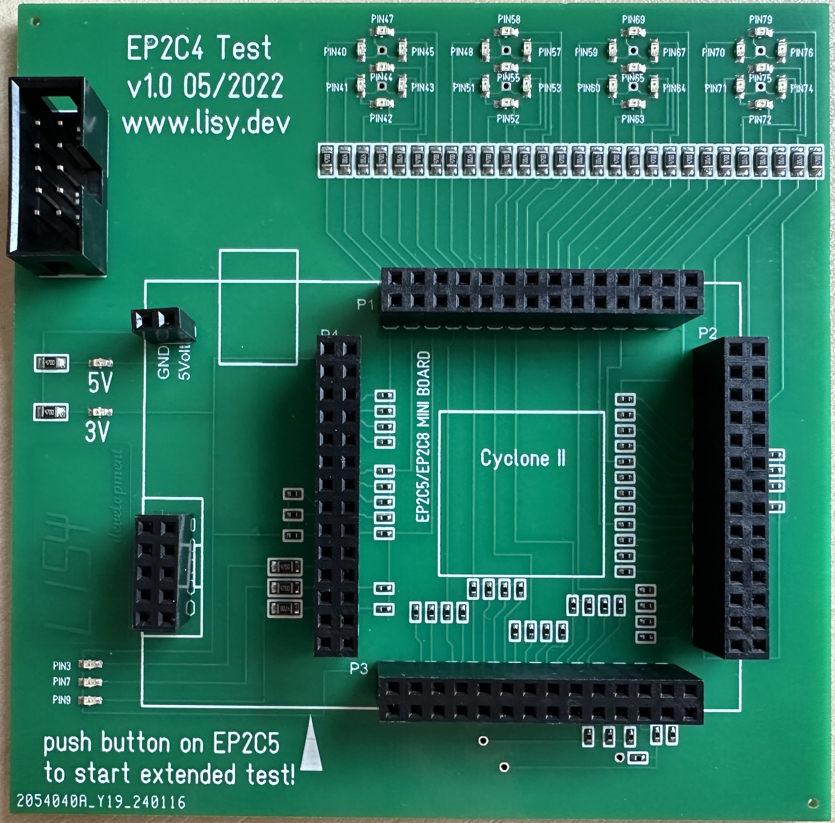
An aside - A FPGA Module Tester
Board
Given the number of Development board
failures that I had experienced, I had toyed with the idea of
trying to create a diagnostic board. Again, I was pleasantly
surprised to find that Ralf had already done exactly that and
posted the
design on his website with examples of the test output for
good and faulty boards. In summary, the board includes 28 SMT
LEDs laid out such as to create faux 4 x 7 segment displays. The
board first tests these 28 outputs, then uses them to report
failures should exercising all of the I/O reveal any faults.
I decided that this would be a great tool
to test any FPGA modules that I might get fabricated as well as to try
and reveal the exact issues with the faulty modules that I had
on hand, and hopefully, be able to detect, and ultimately repair, the hidden
defects.
When Ralf
had the board fabricated, he already had a supply of the
required pin headers, so his BOM did not include them.
However, he kindly created a BOM for me with the headers
and I used it to get some tester boards fabricated by
JLCPCB.
This image is the JLCPCB representation
of the
Gerber files that I uploaded with my order.
(JLCPCB charge a little more for the "hand soldering and
manual assembly" of the through-hole components, such as
the headers, but the convenience far outweighs the
small additional cost.) |
 |
The
minimum PCB order was 5 pieces but you can choose to
have a smaller number assembled, with a minimum of 2.
Although I wasn't going to need 5 of these, since
the biggest elements of the cost were shipping and VAT,
I chose to have all 5 assembled anyway. (The extras are
available for sale if anyone is interested.)
Ta-da! - One of the assembled boards, ready to test my
faulty FPGA boards. |
 |
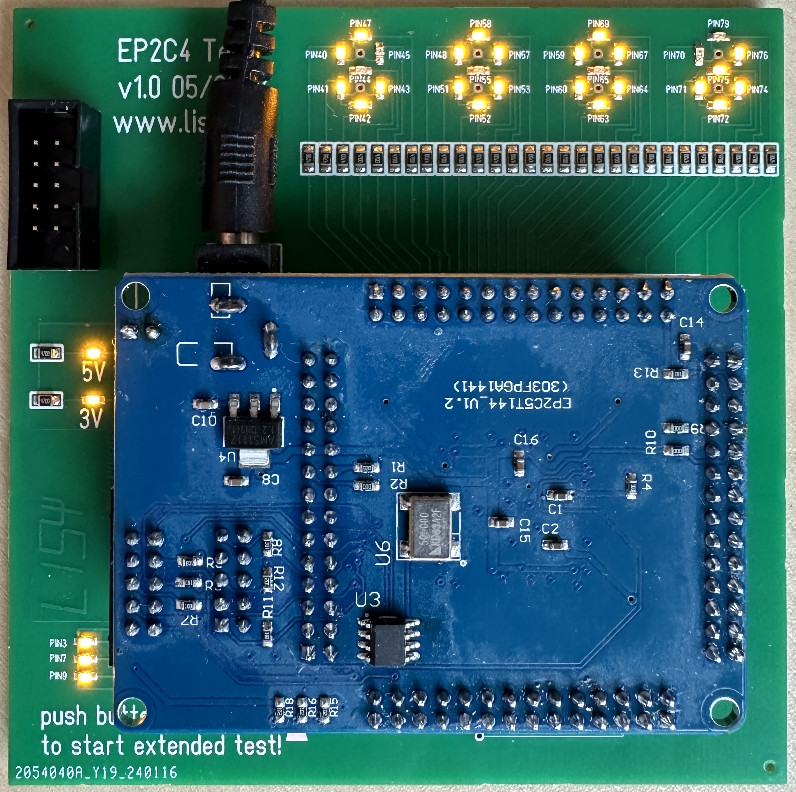
The tester
board has already proven its value!
One of my
previously faulty boards, now testing as "Good". When
first run through the tester, the diagnostics identified
that Pin 8 was reading "low" when it should have been
"high". (Pin 8 is used by MFX to enable reading of the
VRAM.)
Although I had previously examined this
board under a magnifying glass, I had not spotted any
obvious errors. When the tester found an issue with Pin
8, I managed to reflow the FPGA pin which was enough to
repair the fault. |
 |
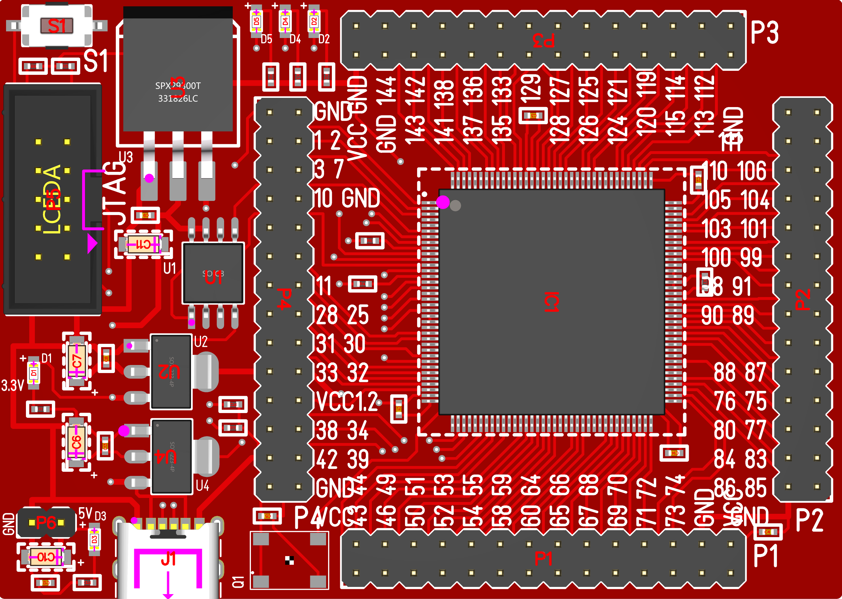
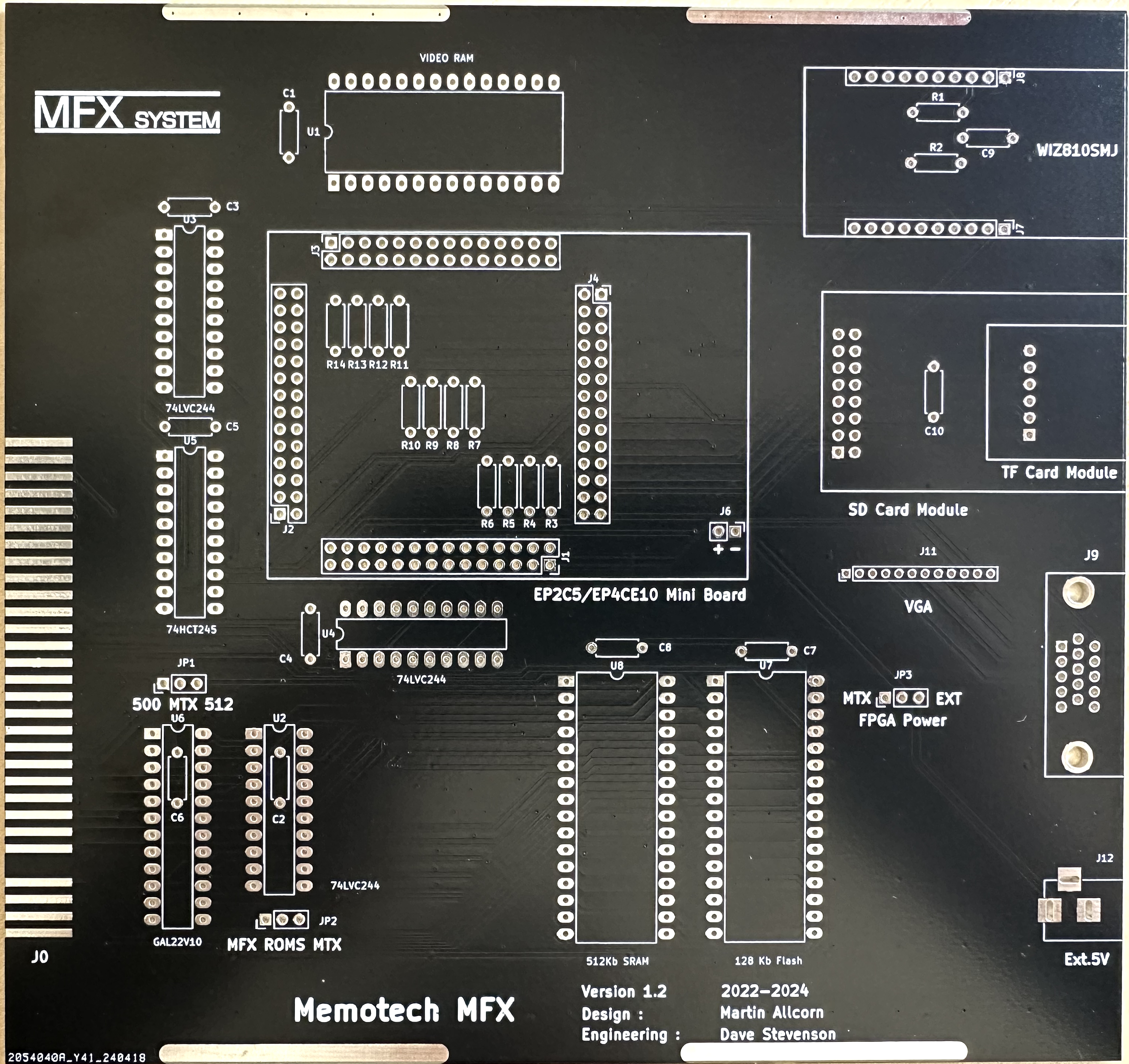
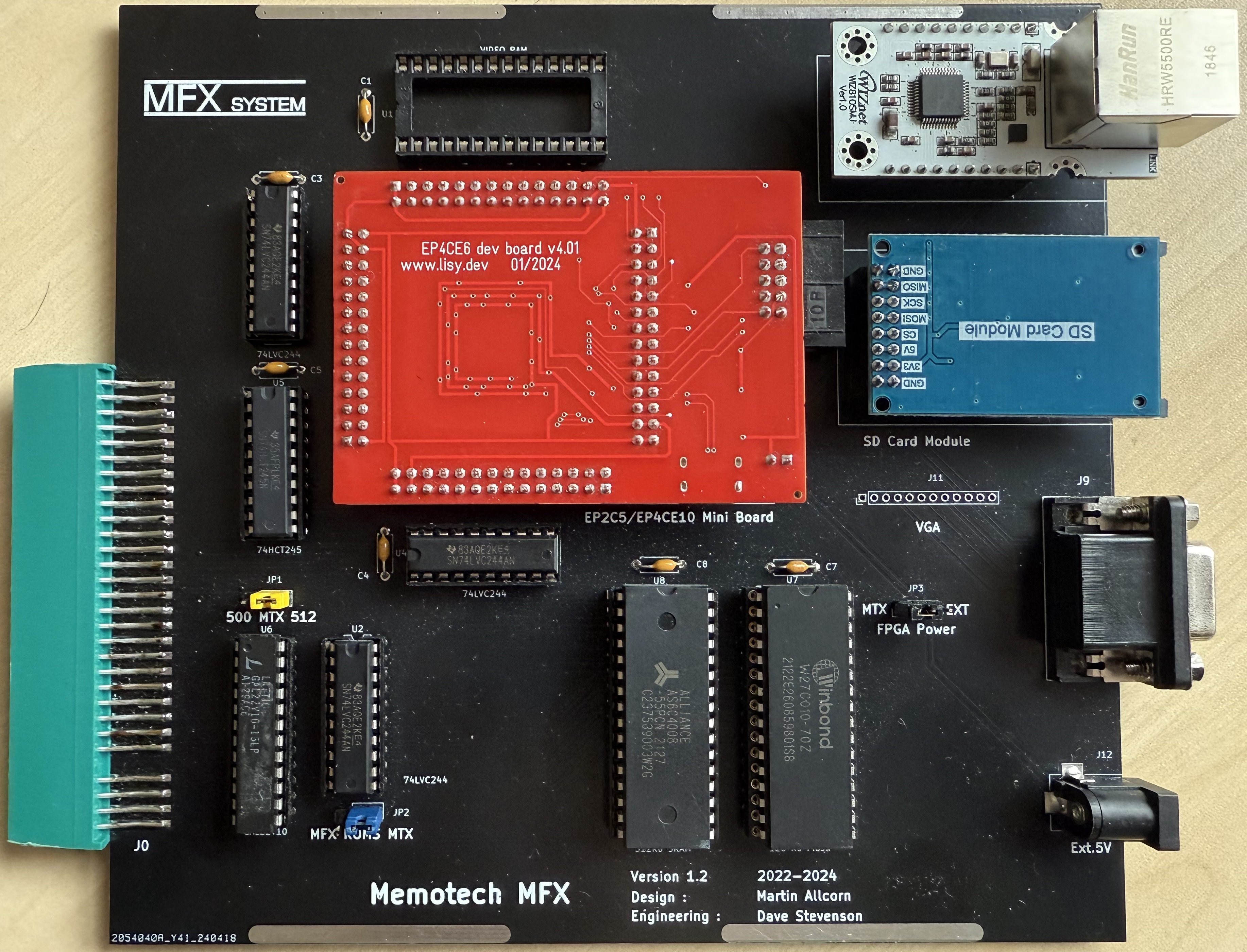
Replacement FPGA Development
Board
The original Cyclone II development board
was designed to cater for the use of EP2C5 and EP2C8 devices
(although all of the boards I've seen appear to have been fitted with
the EP2C5). Since the EP2C8 has 4 fewer I/O channels available
in the FQFP package, the corresponding four pins (26, 27, 80,
81) on the original development board were tied to either 1.2v or ground
via 0 ohm resistors. Another pin (73) was connected to Vcc and
ground for use as a power up reset and one pin (17) was
connected to the 50MHz oscillator, making the signal available
for external use.
These "dedicated" pins could all be
repurposed and used as normal I/O by removing the extra
components and connections. For MFX, we didn't do this to avoid
having to modify every development board before use and
invalidating any warranty in the process.
Ralf's Cyclone IV board has omitted these
unnecessary components, meaning that it has an additional 6 I/O
pins available on the same headers should we chose to modify the MFX design in
future.
(The three pins connected to the onboard
LEDs (3, 7, 9) and pushbutton (144) have not been modified.)
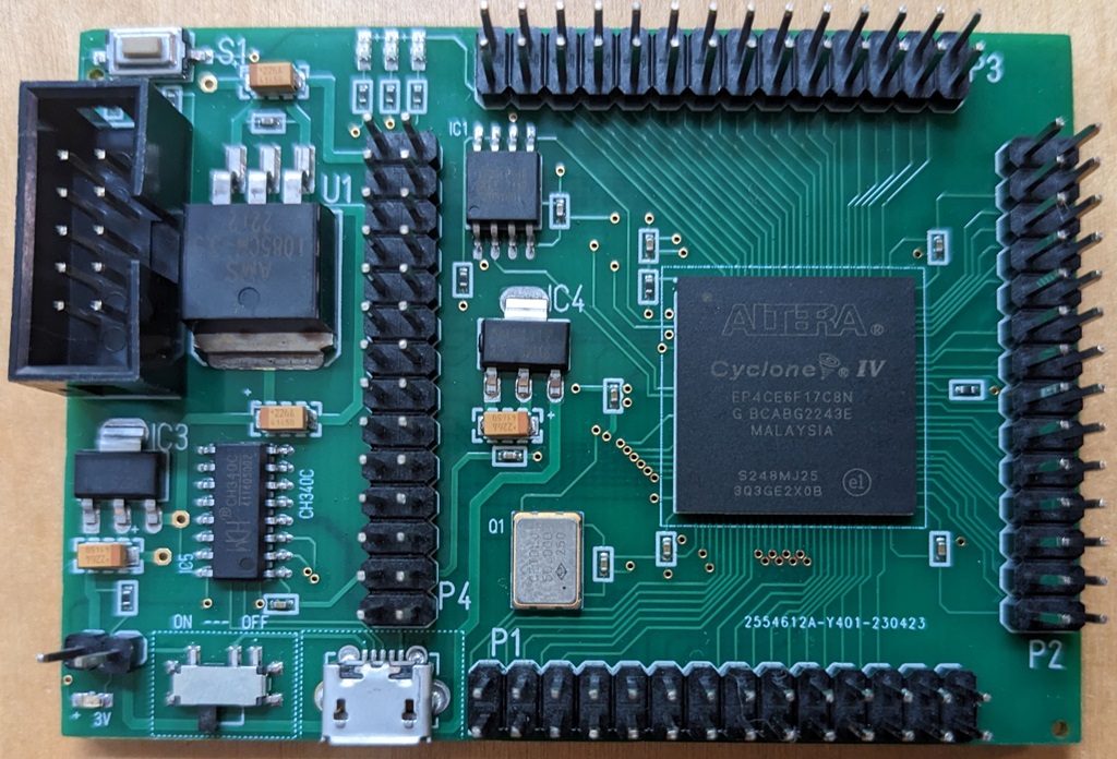
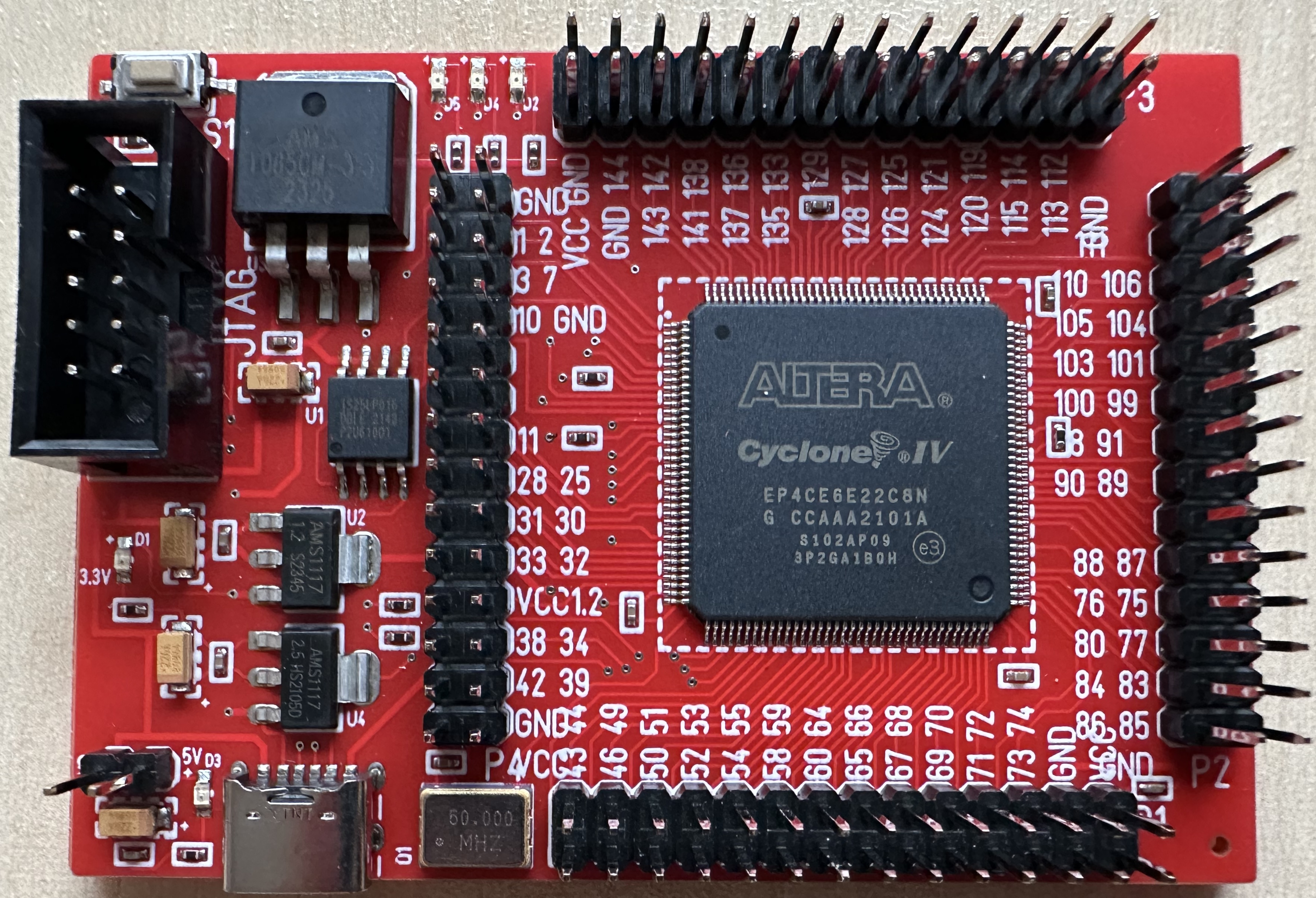
The Cyclone IV is not a stock item for
JLCPCB, so I first needed to pre-buy some chips and store them
in my personal inventory before the boards could be ordered. The
price of the parts is initially estimated and you pay that
estimated price when the parts are ordered. The estimate was
quite expensive, but thankfully, when the parts arrived, the
price did drop, though I ended up having to pay currency charges
to my credit card for both the initial purchase and the refund.
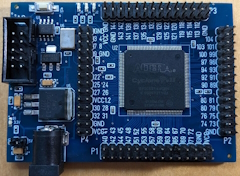
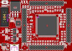
The JLCPCB
representation of the assembled board.
I thought
that it would be a good idea to make the Cyclone IV
board markedly different to the Cyclone II, so, going
with a Memotech flavour, I chose the red PCB colour. I
think that it will look awesome if I make future runs of
the MFX PCB black! |
 |
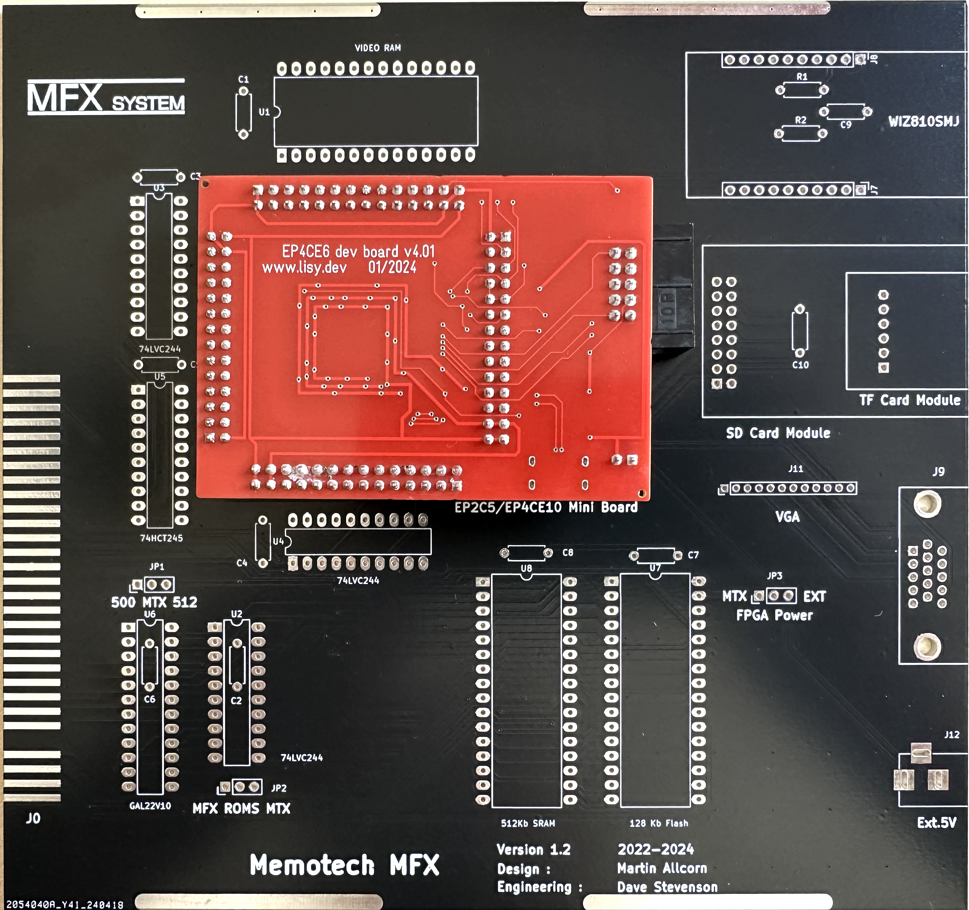
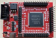
One of the
first batch of PCBs back from JLCPCB.
Loaded with
a copy of Ralf's updated test program for the EP4CE6,
the board passed testing with the Tester board. The next
step would be to load the MFX application and see how it
fared. |
 |
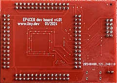
Solder
side of the PCB.
As noted above, there are no
components on this side, this slightly reduces the cost
of manufacture. |
 |
Converting the MFX FPGA firmware to Cyclone IV
When the target device is changed in
Quartus II, the pin assignments are reset. The best way to
mitigate this is to copy the existing Quartus project into a new
one and export the assignments before changing the FPGA type.
Ralf created a script file that processed the exported
assignments and remapped them for the new FPGA pin-out. After changing
the FPGA type, the remapped assignments could be imported back
into the new project.
The MFX application recompiled without
error, but a number of warnings were issued related to the
memory configuration. The Cyclone II can configure the memory
bits as M4K memory blocks (each block being 4k bits) which have been superseded by
the M9K memory type (each block being 9k bits ) in the Cyclone IV. Although the compiler
converts the memory type without issue, the M9K type is ideally
suited to the configuration of RAM with 8 data bits and 1 parity
bit and some of the MFX memory programming may benefit from
being modified to use new memory type. However, since the
internal structure is essentially an array of single bits, it
may make little difference, other than to perhaps code
readability.
When the project is compiled, Quartus II produces .pof
(Programmer Object File) and .sof (SRAM Object
File) files which are used in ASP (Active Serial Programming)
mode. After compilation, it is necessary to use the File
Conversion utility to create the JTAG .jlc
(JTAG Indirect Configuration) file used to program the EPCS16
serial configuration device on the board. (Serial configuration
devices are flash memory devices with a serial interface that
can store configuration data for FPGA devices that support
active serial configuration and reload the data to the device
upon power-up.)
The Cyclone FPGA supports various output
pin current drive settings that can be configured to meet the
specification of the connected logic devices and to reduce
system noise. The available settings for each pin depend on the
physical location that the pin occupies on the package. The
tables below are extracted from the Cyclone Handbooks, the
available current settings for the EP2C5 are shown one the left
and the available settings for the EP4CE6 are shown on the
right.
In both cases, the default current
strength setting for a particular pin is the maximum available
setting for the I/O standard and pin position.
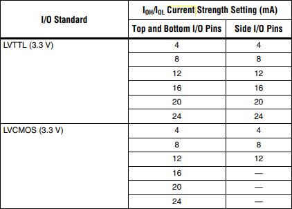 |
It can be seen that the available drive currents for
the EP4CE6 are much reduced from the EP2C5 |
For MFX, the FPGA is interfaced to both
3.3V LVTTL and 3.3V LVCMOS devices and during development, it
was found that the output drive currents had to be reduced to
the minimum in a number of cases to increase the stability of
the system, so the reduced drive currents available in the
Cyclone IV E were not expected to present a problem..
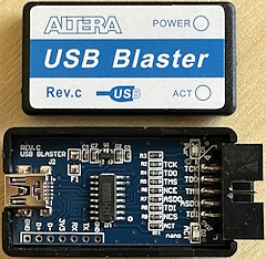
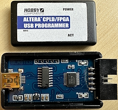
Programmer Issues
I was able to program the device in JTAG
mode using the same cheap USB Blaster clone that I used to
program the Cyclone II device. This programmer was purchased a
few years ago and works fine in ASP or JTAG mode. However, many
of the programmers that are currently available from China,
though they appear visually identical, reportedly do not work in JTAG mode. Again, Ralf Thelen has
some useful info on
his site about this issue, but in short, most of the cheap
clone devices currently available use a CH552 MCU with an
integral USB host that only works in ASP mode, at least, when
programming Cyclone FPGAs. (These devices don't have a visible
crystal oscillator but the CH552 does have a 24MHz oscillator on
the chip.)
To make sure that it would be possible
for others to program the Cyclone IV board, I bought a bunch of
the generic USB Blasters from AliExpress which turned out to be
the CH552 model and, as expected, did not work in JTAG mode, the Quartus II
Programmer utility failing with the message "209040
Can't access JTAG chain", so I needed to find an
alternative.
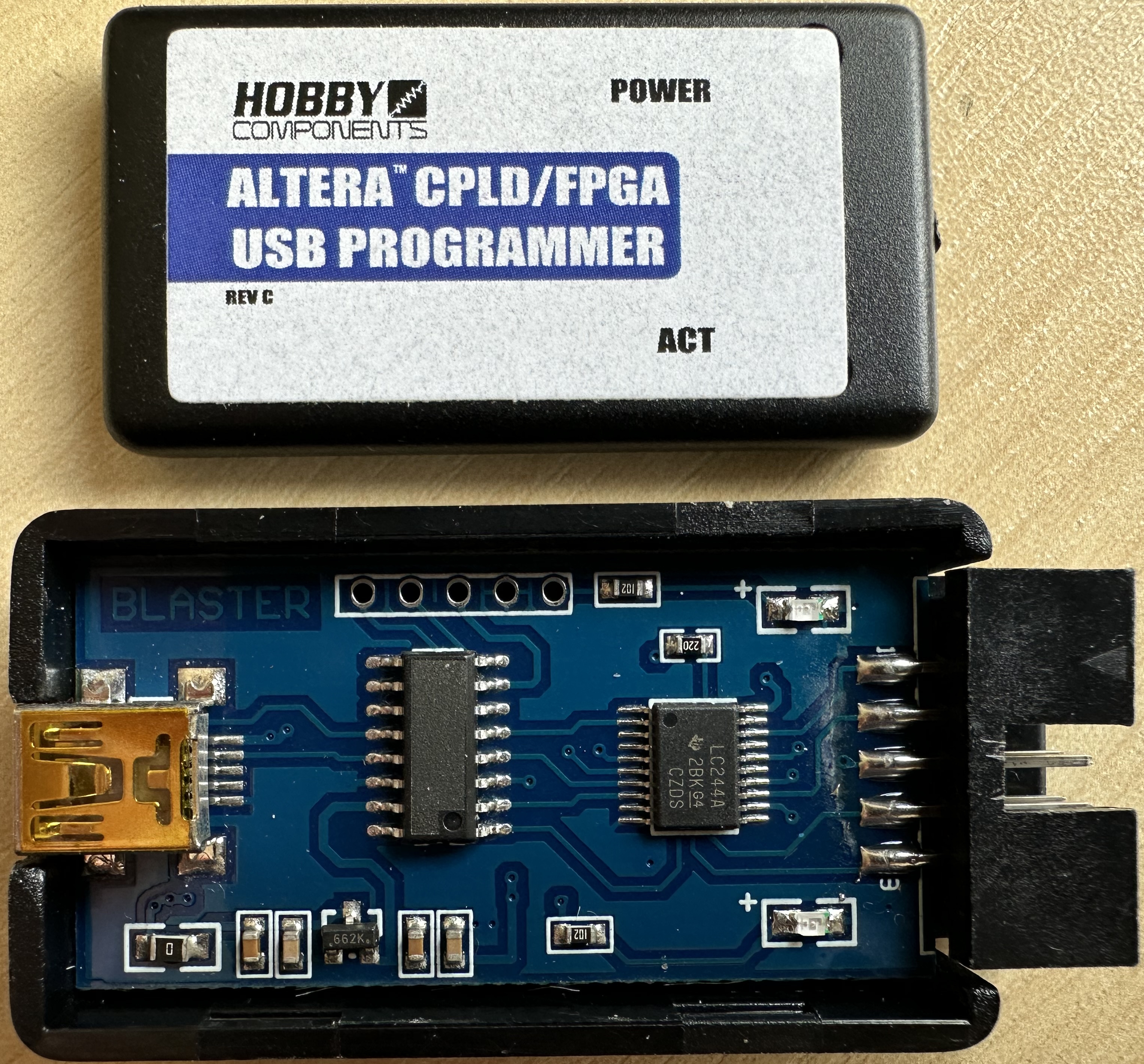
Martin bought his original Cyclone II
development board from
Hobby Components, along with a Hobby Components "Altera
FPGA/CPLD USB Programmer". The package looks identical to
the other USB Blaster clones apart from the Hobby Components
label. These devices are still available and listed on their
website as "USB Blaster compatible" and, having some confidence
that the claims made on a UK website would have some worth, I
bought one of these to test and confirmed that it did work in
both ASP (with Cyclone II) and JTAG (with Cyclone IV) modes.
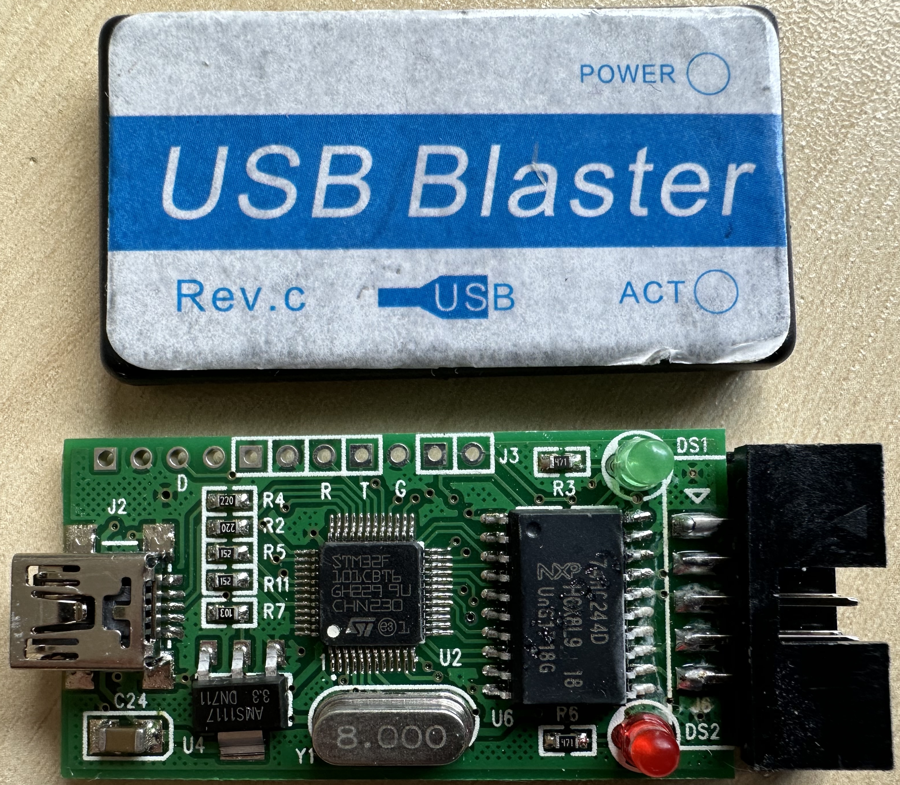
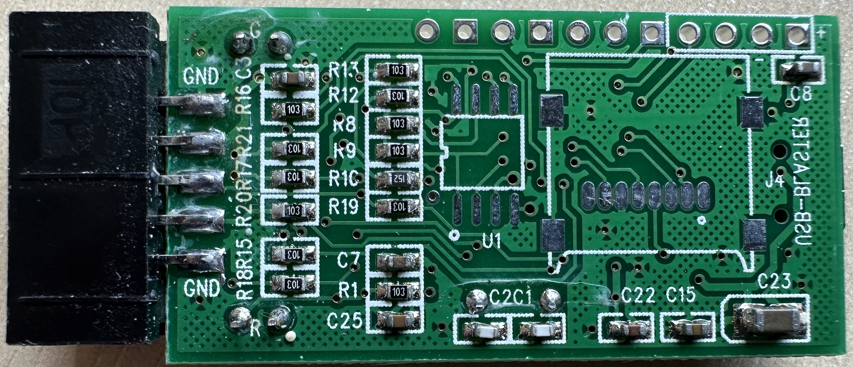
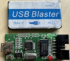
I
inspected the internals of the three devices that I had
tried . . .
The major components in the cheap
clones from AliExpress were the CH552 type, with
resistors on the outputs to the JTAG lines.
The
rest of the components are a 662K LDO regulator and
supporting capacitors to step the 5V USB voltage down to
3.3V for the FPGA.
There are no components on
the reverse side of the PCB. |
 |
My
original programmer was identical to the STM32 device
with the green PCB on Ralf's site, including the STM32,
8Mhz oscillator and HC244.
(All of the working
Blasters on Ralf's site include a '244 (level
shifter/buffer) on the outputs to the JTAG lines - could
that be the difference?) |
 |
| The
reverse side of the PCB has quite a few passive
components fitted, including the capacitors for the
AMS1117 3.3V LDO regulator and resistors on the JTAG
lines. |
 |
The Hobby
Components device was much more basic than my old
version, the layout was very similar to the AE clones,
it had a 16 pin chip that had had its surface etched to
remove its identification.
I suspect that it
probably did use a CH552 as there was no external
oscillator fitted and the chip footprint was the same.
However, there was a LC244A fitted on the JTAG lines.
(NB: Bill bought a Blaster from
Hobby Components some time ago, it did not work at all.
It used a PIC18 but was of a different design to the one
on Ralf's site.) |
 |
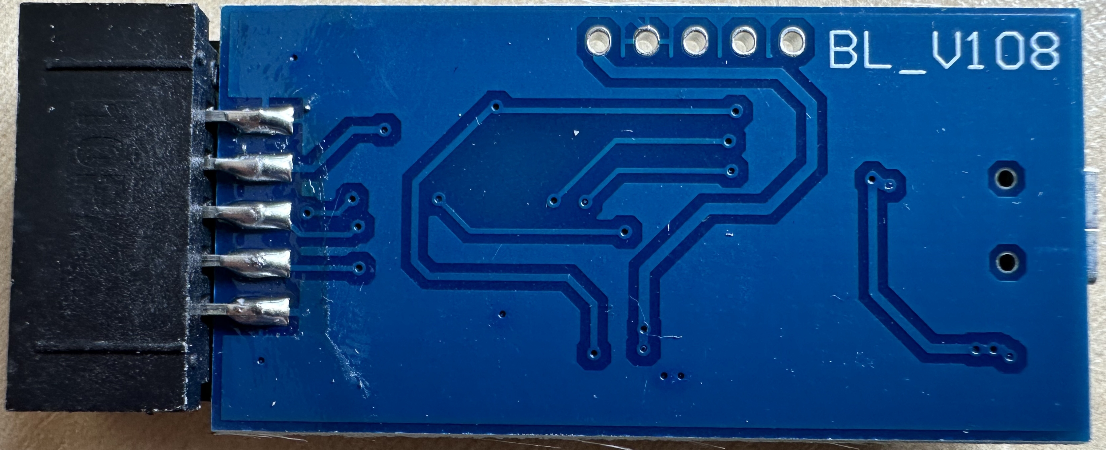
| There are
no components on the reverse side |
 |
The
FAQ on the Hobby Components support forum advises that the
programmer "is not a general purpose JTAG programmer and
will only program Altera devices in the supported list".
This may help explain why so many of the USB Blasters are
advertised as being JTAG compatible without being swamped with
returns (maybe they are?); perhaps they are capable of being
used with other, non-Altera devices to the purchaser's
satisfaction or the buyers are only using ASP and don't
encounter the JTAG issue?
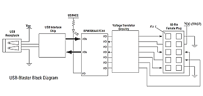
The other solution known to work is the
Waveshare
USB Blaster V2. These devices are available from Amazon but
in the UK cost around £35 - about 3x the price of the Hobby
Components version. This device uses hardware much closer to the
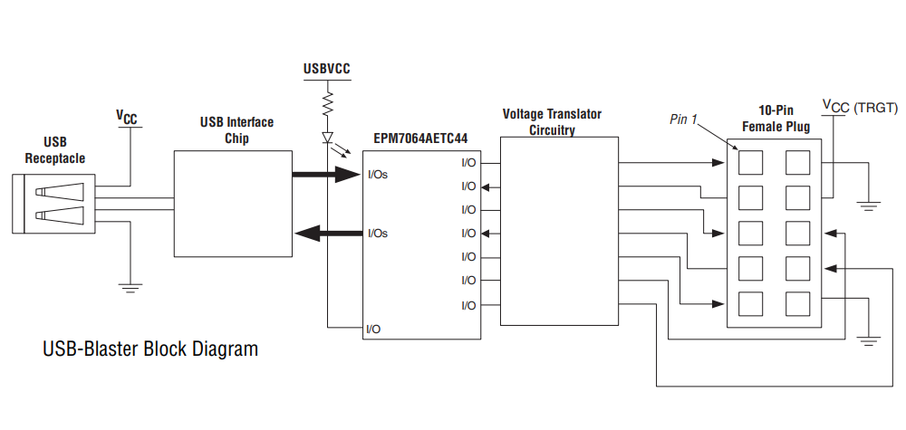
original Altera device, i.e., a FT245 (USB interface), a CPLD
(an Altera EPM3064A) and a 244 (LVC244A) buffer/line driver.
It seems probable that the reason the
very cheap clones don't support JTAG is the use of simple
resistors, rather then proper level shifters/buffers, on the
outputs. Another possibility is that the clock speed is too high
for the Altera JTAG interface that's supposed to run relatively
slowly (6Mhz). Either way, it doesn't really matter, the
important thing is knowing which ones actually work.
Initial Results
Despite my confidence that the Cyclone IV
FPGA board would work well, initial results were somewhat
disappointing. Whereas the emulated VDP output from the Cyclone
II board produced a crisp, clean, signal on my VGA monitor,
output from the Cyclone IV board produced noticeable "hum bars"
reminiscent of the legacy VDP monitor output. Results appeared
to depend on the VGA monitor being used though, Martin observed
similar results to me using his LCD display while Bill could
barely detect a difference with his LCD monitor and saw no
adverse effects at all with his analogue VGA monitor.
Although this was not a major problem, I
felt any loss of display quality was a step backwards and needed
to be addressed.
A number of theories were discussed that
might explain the issue, including inadequate I/O decoupling,
power supply effects and VRAM access timing.
Although the FPGA board has very few
decoupling capacitors on the I/O lines, there are no loess than
on the Cyclone II board and the Altera Cyclone IV Design
Guidelines (AN592) advises that "Cyclone IV devices include
on-die decoupling capacitors to provide high-frequency
decoupling. These low-inductance capacitors suppress power noise
for excellent signal integrity performance and reduce the number
of external PCB decoupling capacitors, saving board space,
reducing cost, and greatly simplifying the PCB design." Martin
also tried tacking on some additional capacitors which had no
effect on the display quality.
Another thought was the rate at which the
VRAM signals were changing and potential signal slew issues.
There was limited ability to change the signal transition
behavior on the Cyclone IV; the slew rate on LVCMOS pins cannot
be changed from the default. In an attempt to confirm that it
was a VRAM (rather than VGA) signal issue, Martin created a test
build that used internal FPGA RAM, rather than the external
VRAM, as the video data buffer which resulted in the VGA output
being more like that of the Cyclone II board's quality.
However, this could not provide the
final solution as, despite its increased RAM over the EP2C5
(having13kB), the EP4CE6 (with 30kB) does not have enough
available RAM to cater for the expanded video modes created by
Bill (a total of 36kB were required). This left two options,
either drop the enhanced video modes (another retrograde step),
or consider upgrading the FPGA to a higher spec Cyclone IV.
The next model up in the Cyclone IV range
(the EP4CE10) is available in the same pin-out as the EP4CE6 and
includes 46kB of RAM. So, another set of FPGA boards were
ordered with the higher spec FPGA.
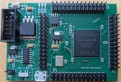
Second
Attempt
When getting a set of boards made with
the EP4CE10 fitted, I also used a right angled connector for the
programming header. Not having the programming header on the MFX
board was a conscious decision when the board was designed. It is
not an issue for users, but does make it somewhat awkward to
reprogram the FPGA during development.
The JLCPCB
representation of the assembled board.
Sticking
with the Memotech Red theme, see how the programming
header now extends to the side of the board. |
 |
Updated
board back from JLCPCB with an EP4CE10 fitted
Unfortunately, I did not check the clearance between the
right angled header and the SD card slot header on the
MFX PCB and
found when the boards arrived, that it would still not be
possible to reprogram the board in situ - oops! |
 |
The good news is that that that board
works well, with all of the required memory now available inside
the FPGA. The change is almost cost neutral; although the larger
FPGA is more expensive, the external VRAM and socket can be
omitted. Getting these boards produced myself will end up a
little more expensive that using the cheap Cyclone II boards,
but the quality and reliability makes the small increase in cost
acceptable (to me anyway).
Form
over Function?
As I mentioned earlier, I thought that
the red FPGA boards would look really cool on a black MFX main
board, so I had a small batch made to check it out . . . .
The bare PCB.
With the ambient light at the time and the
reflections, it's not a great photo, but it's hopefully
good enough to show how nice the black PCB is.
As
an aside, Martin noted how much more difficult it is to
trace the track routing with the copper obscured by the
black mask, but that's not really an issue once the
design has been proven. |
 |
A mock up of
how the final board would look - one of the EP4CE10
modules placed on the PCB.
Do you think that it
looks as good as I do ? |
 |
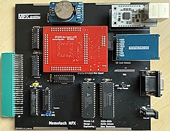
| Fully
populated with MFX components - note the unpolulated
VRAM socket as the external VRAM is no longer required. |
 |
I think that the black PCB with red FPGA
board looks great and matches the colour scheme that Memotech
used for the MTX, it's almost a shame that MFX is hidden inside
the case! In terms of features though, the Cyclone IV version
currently doesn't offer much beyond what the Cyclone II version
delivers, other than perhaps some additional expansion potential. However,
we have been unable to think of anything that can easily be
added to the current design, so, if you have any ideas, let us
know . . . . .
Expansion Potential ?
With the MFX VRAM chip no longer being
required, the 25 FPGA I/O pins connected to the VRAM socket are
freed up and available for other purposes. There was a brief
discussion on the Memotech forum on possible uses for the
additional I/O and logic resources, some suggestions were :-
- Z80 DART emulation to facilitate adding RS232
connectivity
- Floating Point Accelerator (as in REMEMORizer)
- Additional monitor support to allow simultaneous VDP and
80 column card output
- Direct Memory Access (DMA) between the SD card and the
Z80
- Upgraded sound output
- A to D / D to A interfaces
- Digital I/O (GPIO) chip
- Real Time Clock (RTC) chip with battery back up
The majority of these ideas would require changes to the MFX
PCB but using the connections to the VRAM socket there are some
possibilities, albeit that, since there are no level shifters on
these connections, anything connected to the VRAM socket pins
needs to use the 3.3VDC levels used by the FPGA.
The simplest, and potentially most useful, modification is
probably a Real Time Clock. Martin had bought some 3v RTC
modules based on the DS3231 and made a small adapter board to
connect it to the VRAM socket. He modified the FPGA code to
support the RTC and added USER commands to the MFX ROM to
facilitate its operation from MFX BASIC.
Having the RTC opens up other possibilities, including the
option for Bill to enhance his FATCOPY program to include
time-stamps when creating files on the FAT partition. Going
further, if CP/M 3 was ported to MFX, file time stamps would be
possible on the CP/M side too.
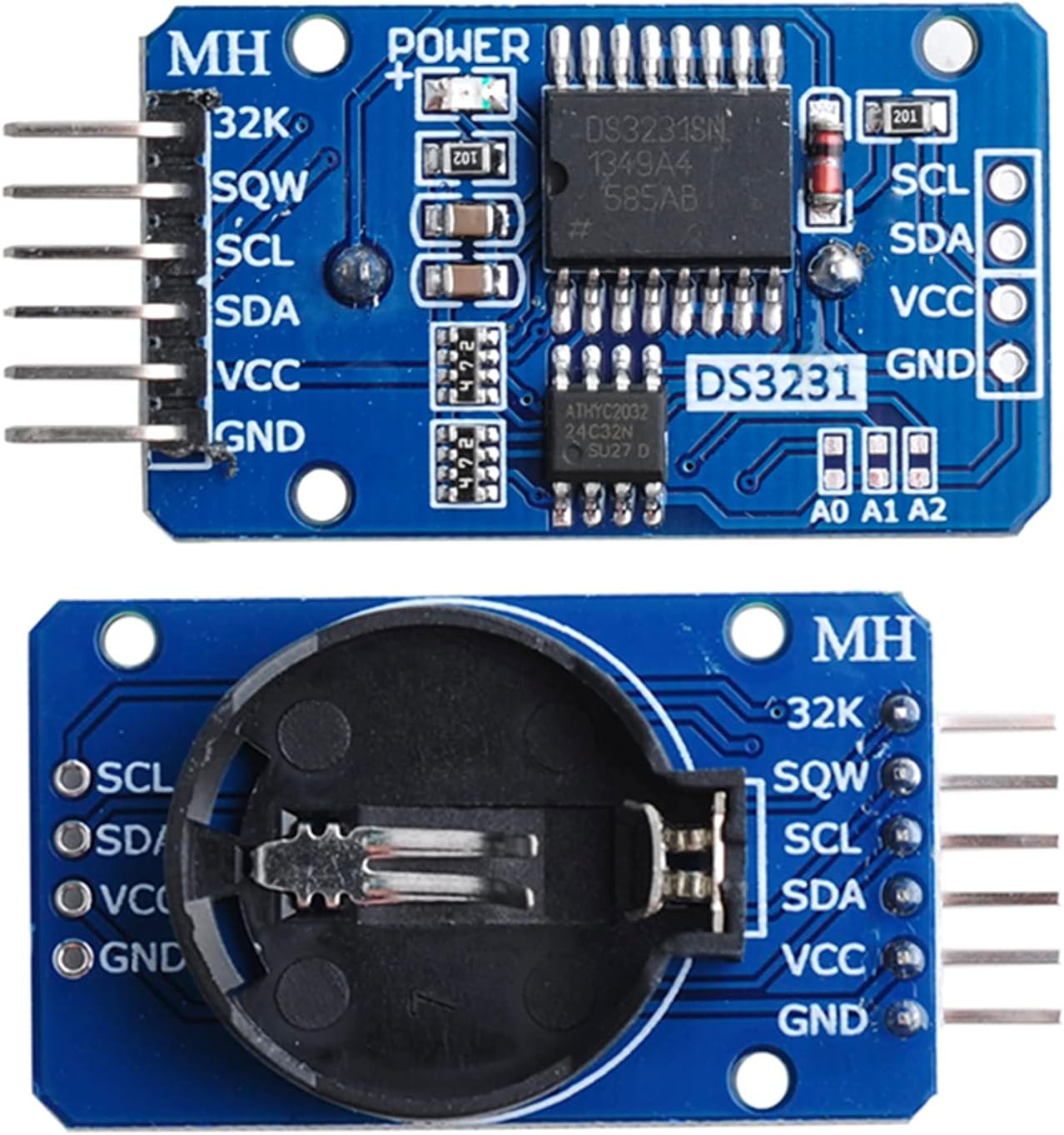
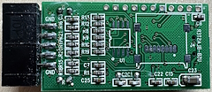
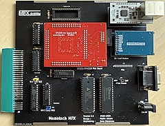
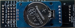
The RTC
module shown here is widely available from many sellers
with quite a few different product labels such as MH,
ZS042, SPX, etc. but the design is the same.
The
main components are a DS3231 RTC and a AT24C32 EEPROM
chip. The modules are typically advertised as being
suitable for 3.3V or 5V operation.
They may be
supplied with a CR2032 non-rechargeable coin cell, a
LIR2032 chargeable cell, or no cell at all. |
 |
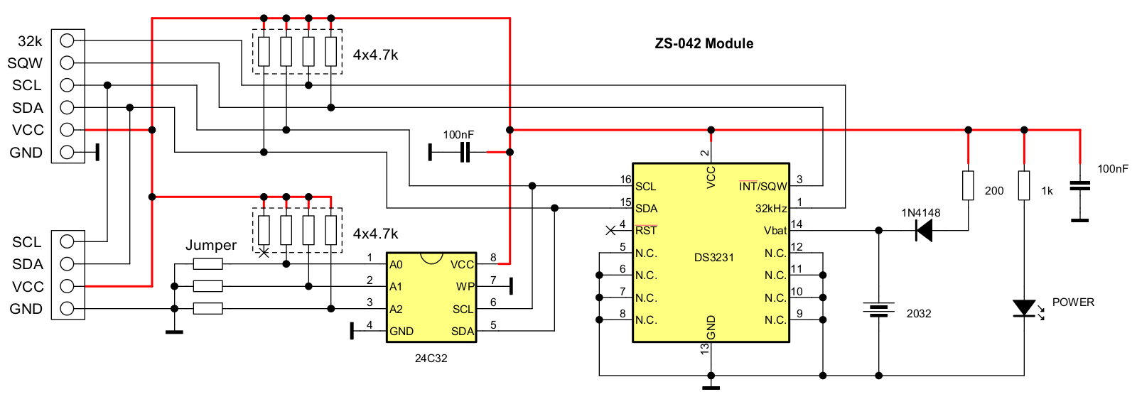
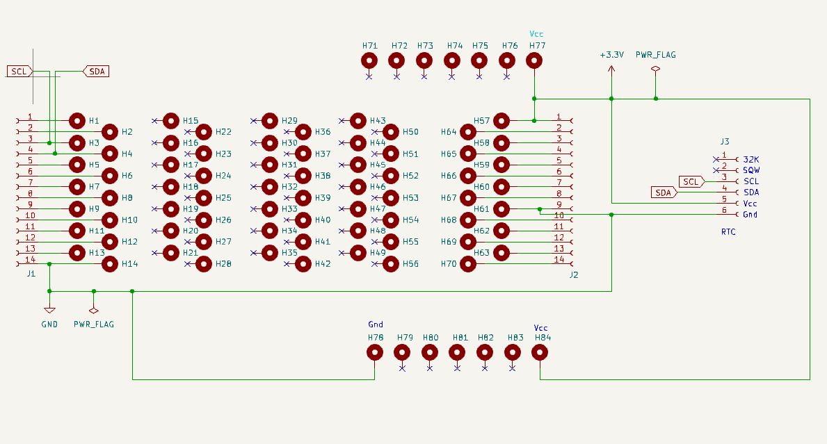
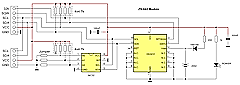
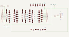
| The
schematic for the RTC module is shown here. |
 |
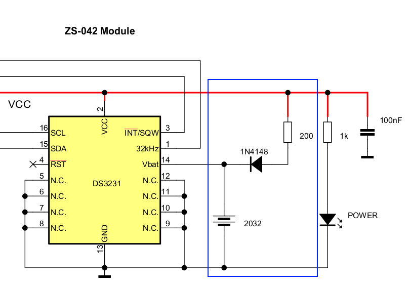
| However,
there is a fundamental flaw in the design of the simple
"charging" circuit. The battery is connected to the
supply voltage through a diode and a resistor, feeding a
slightly reduced supply voltage to the cell - this is a
really bad idea when using a non-rechargeable battery |
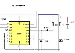 |
Some modules are
supplied with a LIR2032 rechargeable cell, but that is
not a solution to the problem. Using a 5V supply, even
allowing for the presence of the diode, the charging
voltage is slightly too high for the LIR2032. With a 3V
supply, the charging voltage is much too low. So,
there's little point in using the more expensive
rechargeable cell and the best course of action is to
break the connection between Vcc and the cell and use a
CR2032.
The easiest way to prevent feeding Vcc to
the cell is to remove the resistor or diode in the Vcc
line to the cell - the components shown at the upper
right of the photo above. |
| |
|
| To connect
the RTC module to the VRAM socket, I made a "bodge
board" out of a scrap of prototyping board, only
connections to socket pins 28 (Vcc), 20 (GND), 3 (SCL)
and 4 (SDA) are required to be consistent with the FPGA
code. |
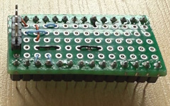 |
| RTC module
mounted on the "bodge board" |
 |
RTC module
inserted in the VRAM socket
Whilst the bodge
board obviously worked, I wasn't very happy sending out
the otherwise "professional" looking MFX with one of
these to enable fitting of the RTC.
I decided to
get some "MFX I/O Adapter boards made. . . . . |
 |
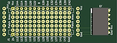
| Although
the RTC is the only expansion curently available for
MFX, I designed the I/O adapter to be able to handle
other options, should they become available. As well as
the hard wired connections to Vcc, GND, SCL and SDA used
by the RTC, the board provides connections to the other
VRAM socket pins and includes a prototyping area. |
 |
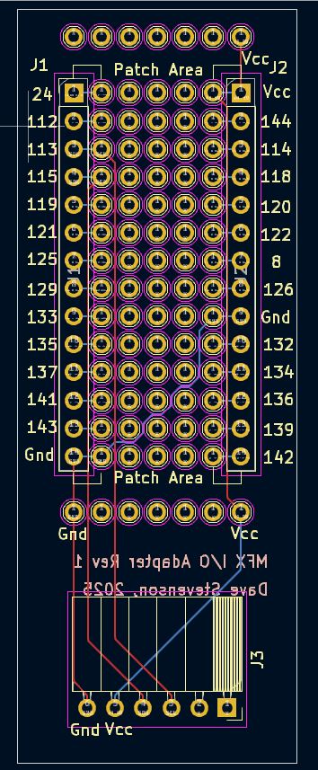
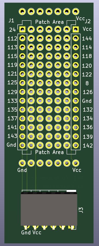
KiCad PCB
view
The PCB design, showing the pin connections,
is here |
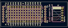 |
| KiCad
render of how the board would look |
 |
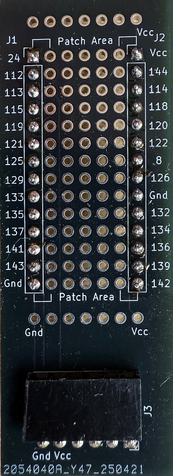
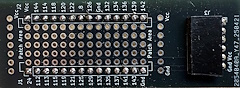
Obviously,
the adapter board needed to be black too :-)
The
completed board, ready to accept an RTC module |
 |
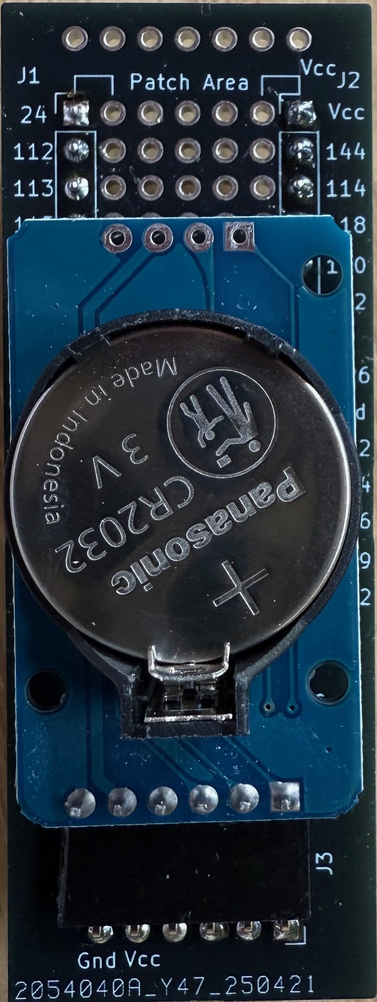
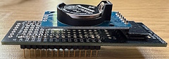
| With RTC
Module fitted |
 |
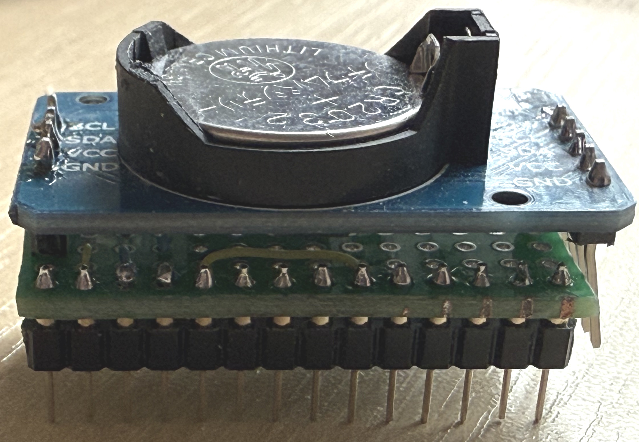
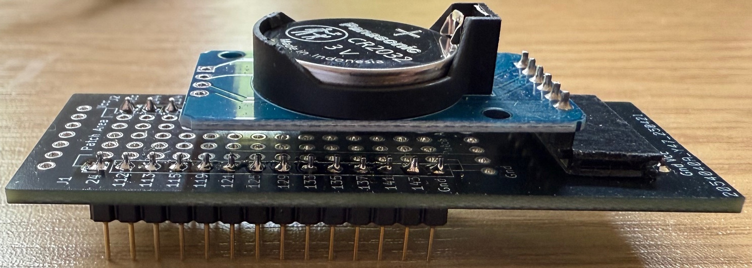
Profile
view.
I am definitely much happier sending these
out with MFX ! |
 |
|