|
 |
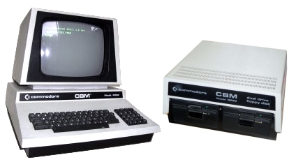
Commodore PET
Projects |
MemoPET
Introduction
MemoPET is a co-processor board
designed for use in
MTXPlus+;
a project developed by Martin Allcorn and myself to build a
"super Memotech MTX". The project is still in the development
stage but three working prototypes have been built and running.
The
system
architecture uses a multi-slot backplane with separate cards
used for the CPU, video display and I/O functions. The core
processor is a Z80 but the system supports co-processors
installed on their own boards. Martin has already designed a
6502
co-processor board that can be used to emulate a BBC Model B
micro.
MemoPET is another 6502
co-processor board, designed to emulate a Commodore PET. Martin
describes development of MemoPET below :
Introducing MemoPET
A 6502 based coprocessor designed for the MTXPlus+. (Other
than ensuring the MTX PSU has enough power the basic design
should also work with the MTX500/512)
Whilst the software is very much work in progress the
prototype board has achieved most of the design goals.
The original 6502 co-processor used a minimal design and
relies on the MTXPlus+ for all of the input/output, the 6502 can
only “see” memory. The new board aims to supply the 6502 with a
limited set of peripherals.
The two biggest I/O bottlenecks are the display and disc
storage, so those I wanted to put on the board. Keyboard and
sound will be passed back to the MTXPlus to deal with.
Originally, I wanted to try a large memory system using the
65816 rather than the 6502, however the extra design
considerations for accessing the extended memory would have
required a completely new OS.
The next option was to go do small memory system like the
Acorn Atom
or
Commodore VIC-20 using the 65816 in 6502 emulation mode.
With a patched version of the original OS to allow access to the
extra memory banks. However, the video hardware on both systems
would have been a struggle to fit into the CPLDs I have
available.
The character based display of the older Commodore PET range
in not unlike the MTX 80 column display, but without the colour
attribute. The VHDL code for that fits the CPLD with room to
spare.
Fitting all of the PET components required for the IEEE
expansion would have required more space than the Eurocard
format allows. However, using the serial IEC port from the Vic
and C64 would fit into the space, at the expense of complicating
the software.
So, the original design had a 65816 CPU, 512k RAM 512k ROM,
along with the external hardware to latch the top 8 bits of the
address bus. The video display needed 2k of dual port RAM and an
84 pin CPLD to generate the VGA timing for the 80 column
display. The display also needs a ROM with the character
definitions . The IEC serial port needs a 6522 VIA.
Since I wanted to try and emulate the 40 column pet display
as well as the larger one, the shift register, colour register
and colour multiplexer are all external components. This leaves
the maximum available space in the CPLD for logic.
VGA at 640x480 specifies a 25.175MHz clock so the board needs
an oscillator, most monitors will lock on to VGA generated from
a 25MHz clock. Since that’s not available from the MTXPlus+
either, I fitted the correct speed part. That needs dividing by
2 to generate the clock for the 40 column display, halving that
again would produce a clock just under 6.3mhz that I was going
to try and run the CPU from.
Communication with the MTXPlus+ required some way to transmit
between the 2 CPU’s Rather than use another 48 pin (and
expensive) dual port ram I decided to use two pairs of 4 bit
registers to allow for 4 byte data transfers in each direction.
Mapping that into the Z80’s I/O map needed a small CPLD even if
there’s available space, and at the time I wasn’t sure there
would be, there aren’t enough pins on the big CPLD.
It took several attempt, but eventually I had a design that
would fit the 19 chips and other parts into the available space.
The Fist 64k of the memory map was designed to be as close to
a real pet as possible.
|
Memory Map of real pet |
|
Proposed low memory map |
| FFFF |
4k Kernal |
|
FFFF |
5.75k ROM |
| F000 |
Remainder of Editor
ROM on
later models |
|
|
|
| F900 |
I/O Area |
|
F900 |
E840VIA |
| |
E880 CRT Controller |
|
|
E8B0 Colour Latch |
| |
E840 VIA |
|
|
E8A0 Comm Regs In |
| |
E820 PIA |
|
|
E890 Comm Regs Out |
| E800 |
E810 PIA |
|
E800 |
E800 Spare |
| |
2k Screen
Editor |
|
|
22k ROM |
| E000 |
12k ? BASIC |
|
|
|
| D000 |
|
|
|
|
| B000 |
4k EPROM Space |
|
|
|
| A000 |
4k EPROM Space |
|
|
|
| 9000 |
Available for Screen |
|
9000 |
Shadow Copy of Screen RAM |
| 8800 |
80 Column Screen RAM |
|
8800 |
80 Column Screen RAM |
| 8000 |
32k RAM |
|
8000 |
32k RAM |
| |
|
|
|
|
| |
|
|
|
|
| 0000 |
|
|
0000 |
|
|
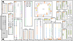
Full 1MB Memory Ma |
FFFFF
F0000 |
Data RAM |
E0000 |
Data RAM |
D0000 |
Data RAM |
C0000 |
Data RAM |
B0000 |
Data RAM |
A0000 |
Data RAM |
90000 |
Data RAM |
88000
80000 |
Data RAM
Low Memory RAM |
70000 |
Data ROM |
60000 |
Data ROM |
50000 |
Data ROM |
40000 |
Data ROM |
30000 |
Data ROM |
20000 |
Data ROM |
10000 |
Data ROM |
00000 |
Low Memory Block |
The extended memory map was kept
simple, and split evenly between ROM and RAM
Initial tests showed issues either
from the wiring of memory, or the memory paging arrangement.
In order to sort determine where the issues were, the board
was re-wired to take the current production version of the
6502, which is the W65C02S.
Dispensing with the 65816 allowed
for the removal of the 2 devices involved in separating the
data bus and upper address bus. It also allowed for the
fitting of a physically smaller 32k ram. A smaller 28 pin
eeprom could have been used but they’re usually slower than
the 32 pin flash devices. The prototype still has a 32pin
device, but only portions of the first 32k are used.
That leaves the board with a just
the low part of the memory map, very much like the original
pet. The major differences are in the I/O area.
Re-wiring for the 6502 helped
identify an issue with the address bus preventing the system
working. At which point I had the basic components CPU, ROM
& RAM connected and working.
Adapting the VHDL display code from
the CFX-3 to produce a mono display with 40 and 80 column
options is more or less complete, allowing for further
testing of the rest of the board. The extra logic to allow
for the separate display opting turned out to only need a
couple of extra macro-cells, however the number of pins in
use means incorporating the external video components isn’t
an option.
The 6502 chip like the Z80 has 2
interrupt pins IRQ that can be turned off in software, and
NMI that cannot. The PET Kernel uses the NMI to trigger the
break process and return to the system prompt. In order for
the Z80 side, which will provide the keyboard support to be
able to support this, a extra pin from the second logic
device has been programmed to issue a short pulse when a
designated I/O port is accessed.
The other interrupt supports both
the 50/60hz system counter and the 6522 VIA, so the
interrupt out from the VIA has to be connected to the CPLD
where it can be mixed with vsync and passed to the CPU.
2 way communication with the Z80 CPU
to provide keyboard input has been incorporated into a
modified pet “Editor” rom. The Z80 side is currently a short
basic program that scans the keyboard on request. That’s
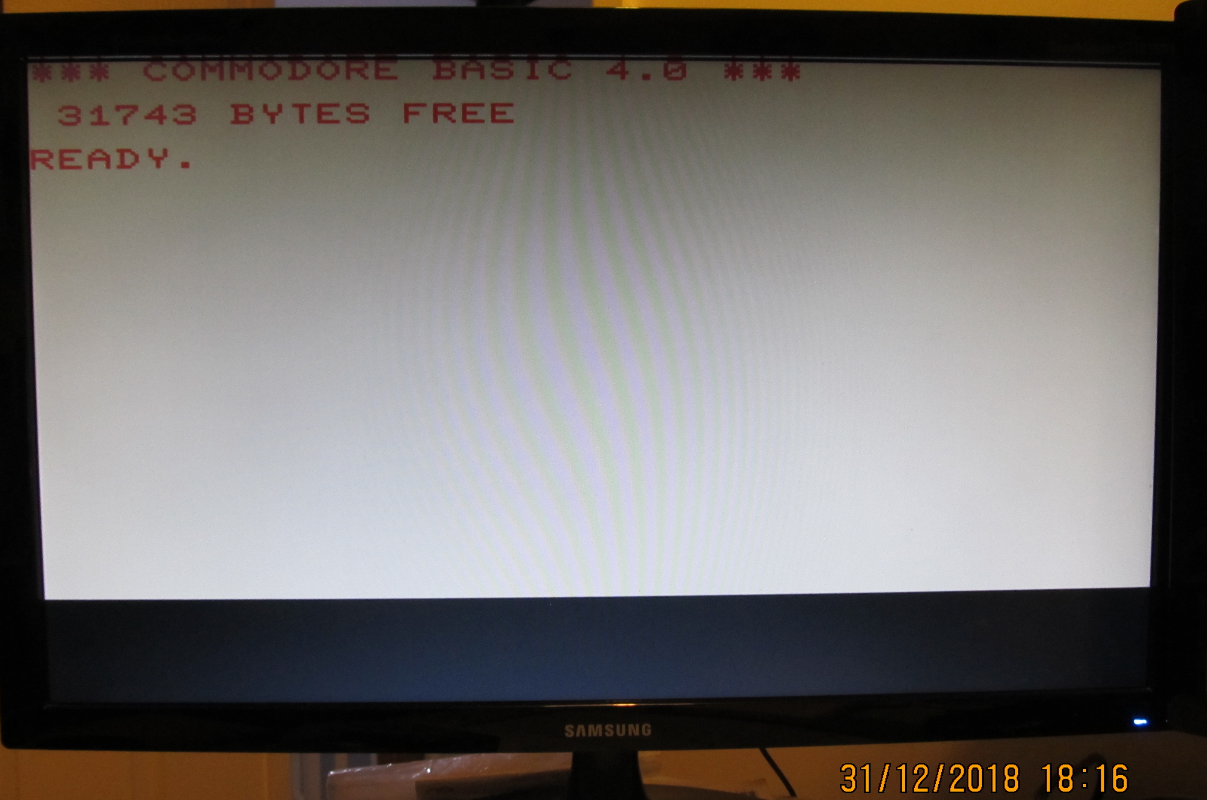
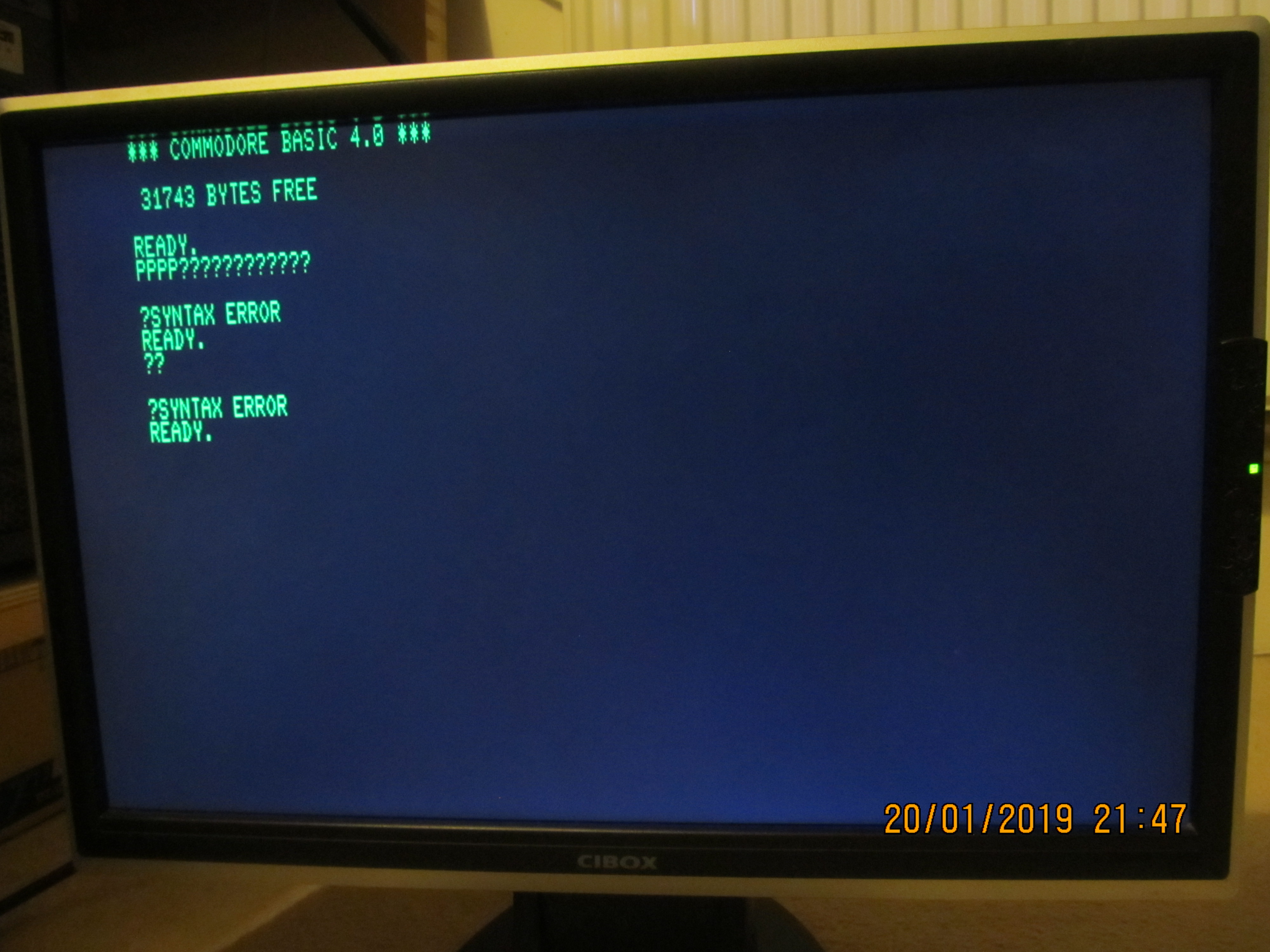
enough to type in and run short programs in Commodore Basic
4 on the MemoPET board.
The board itself beats expectations
for the speed at which it will run at. It has shown no signs
of instability when running off the 12.6mhz clock intended
for the 40 column VGA display instead of the 6.3 clock I had
intended to use. Part of this may be the decision to use the
6502 in place of the 65816 so for now there are no plans to
revert back to the bigger chip, the Memopet will retain the
older CPU and smaller memory map.
On thing that hasn’t be successful
so far is the IEC interface, the timing for the serial
interface is entirely done in software and to date I’ve not
managed to get the board to connect to any IEC peripherals.
To try and get to the bottom of the,
I’ve built an additional clock board that plus into the
sockets freed up by the 65816 to 6502 re-wire. That clock
runs at the same frequency as the clock in the Vic20 so
while further code testing takes place the IEC code from the
Vic can be used without needing to “tweak” the timing
delays.
Merging the IEC code into the Pet
ROMs still needs to be done and that is the next task. That
needs more investigations of exactly how the Pet handles the
IEEE interface so could take some time.
|
|
|
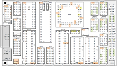
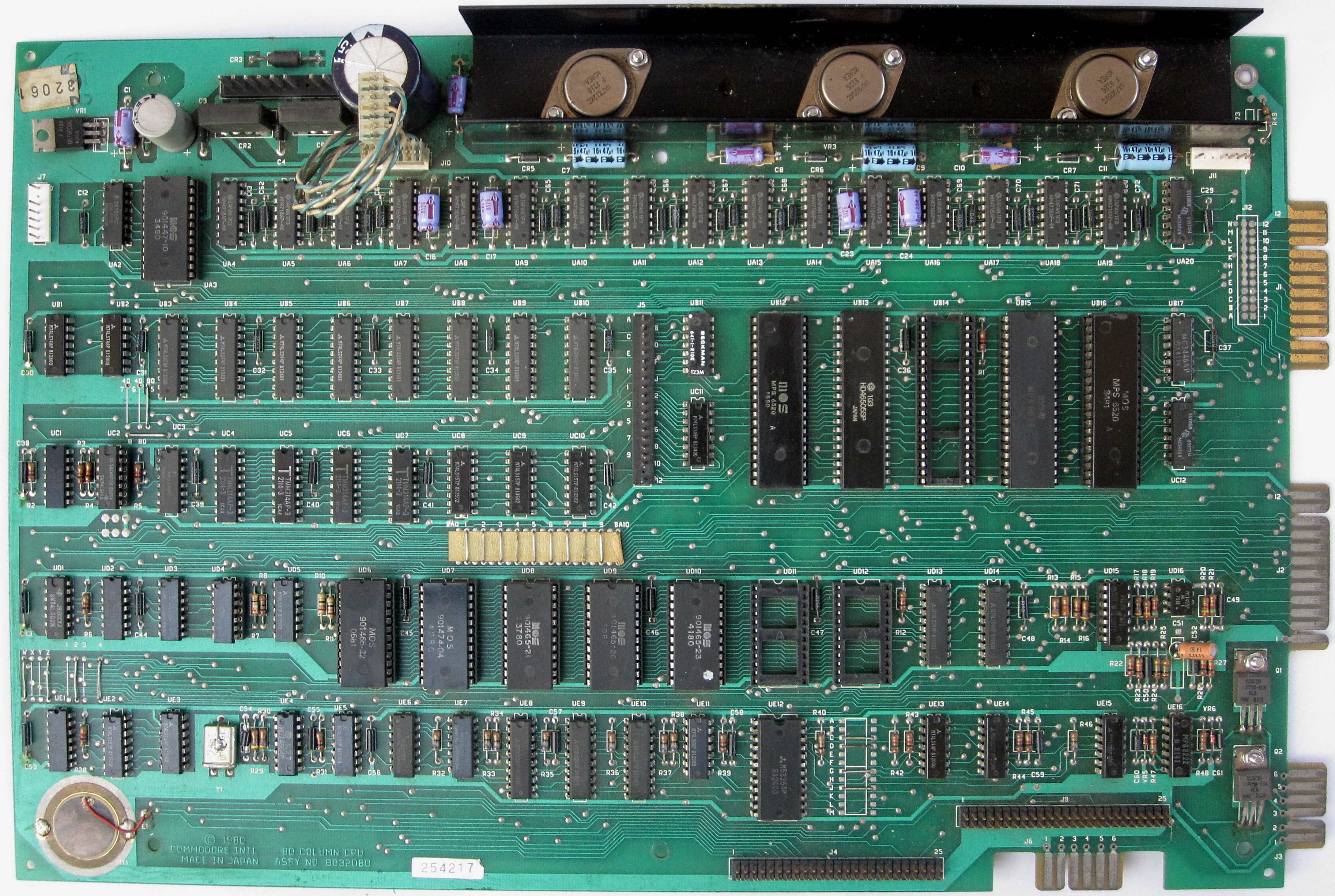
An early version of the schematic that Martin
produced before starting to wire the prototype
- as usual, Martin used Excel to do the layout,
the components are viewed from the solder side.
Click on the image to see a PDF with more detail |
 |
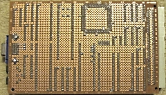
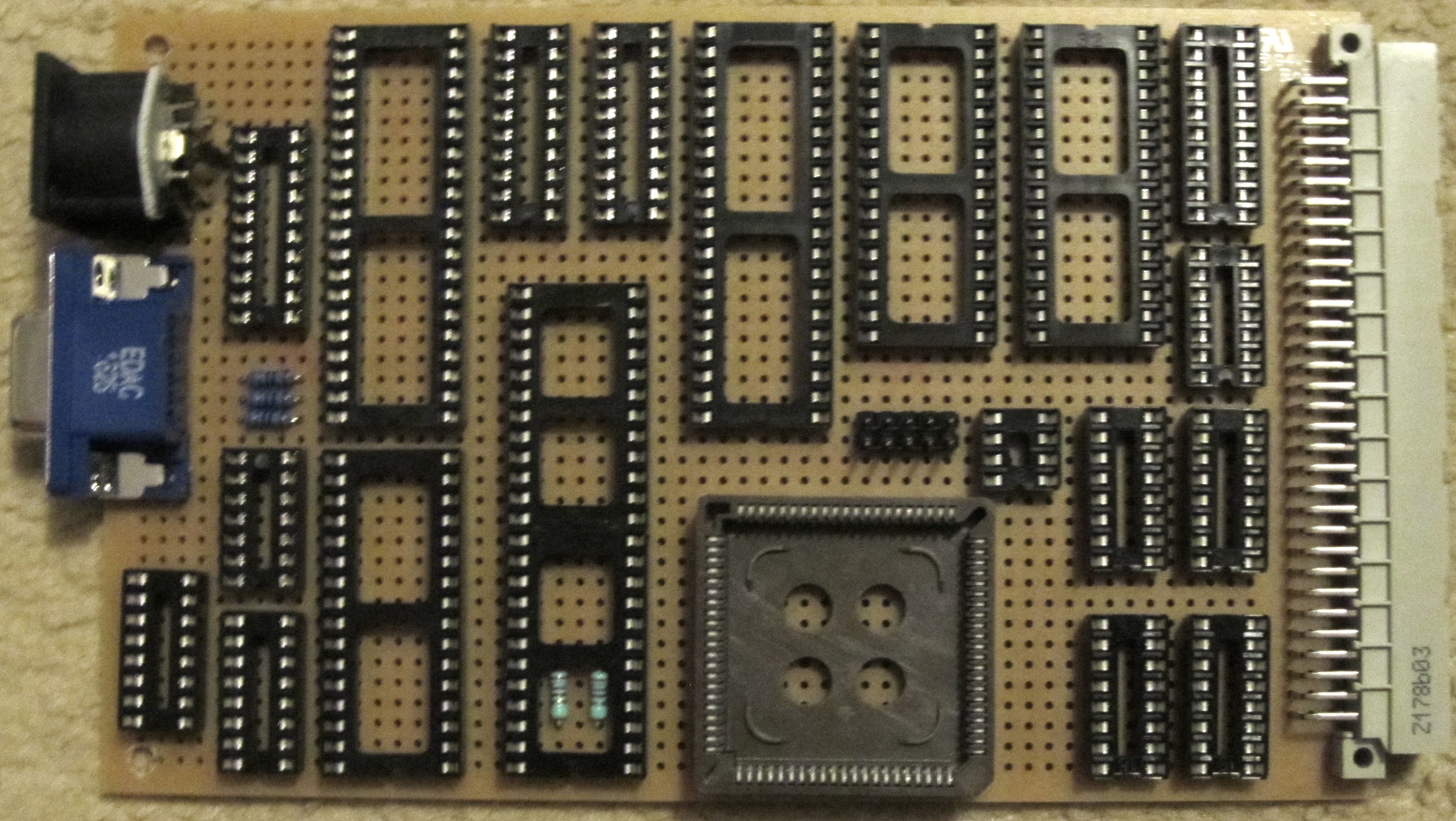
First build of the prototype board, with the sockets
placed, ready for wiring.
It may be of
interest to note Martin's preference for single
sided boards. He feels that they are easier to
solder, though less heat tolerant than double sided
proto boards. |
 |
|
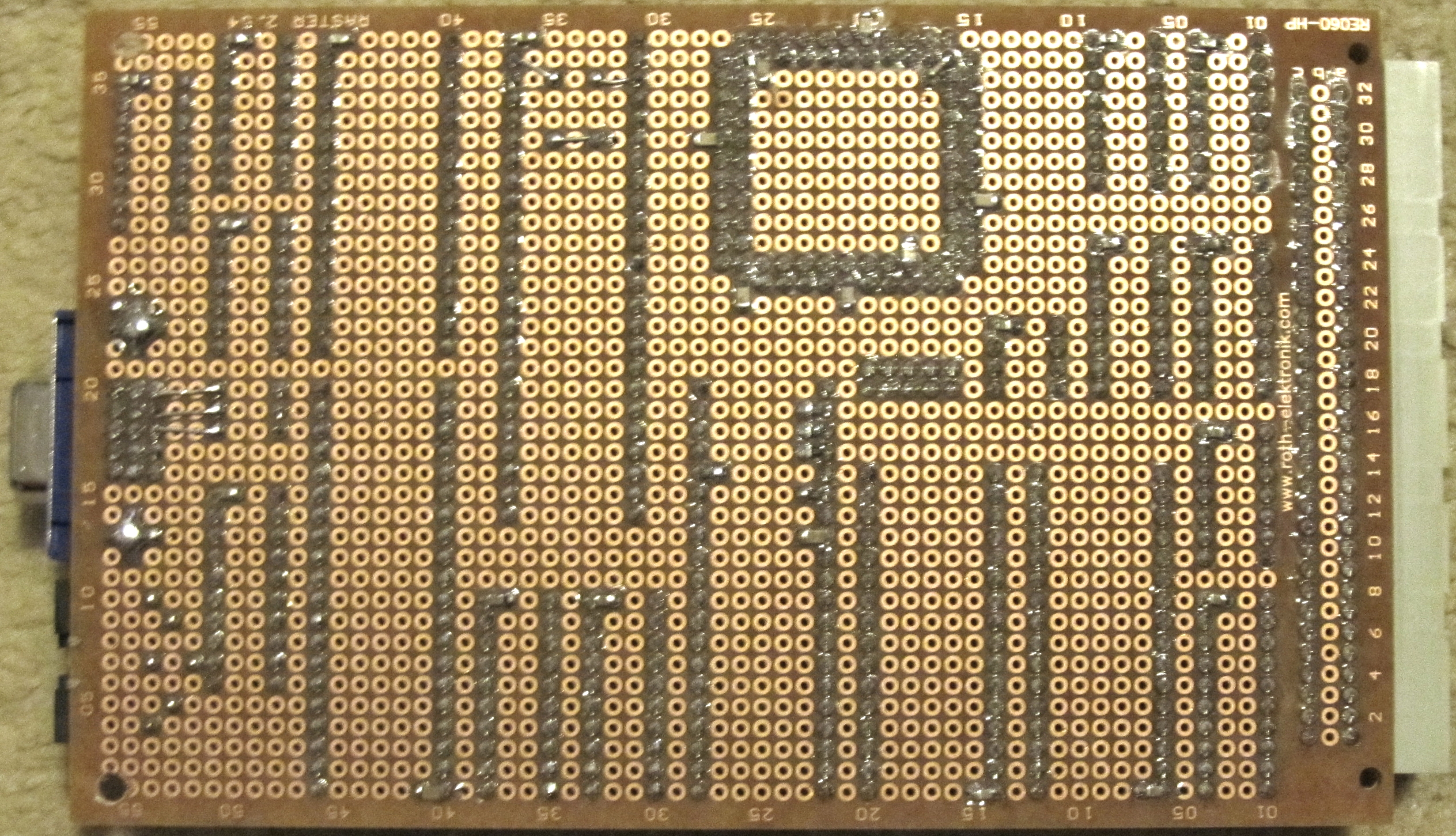
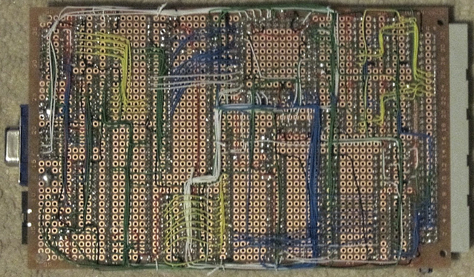
Solder side of the board at the same stage |
 |
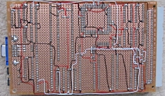
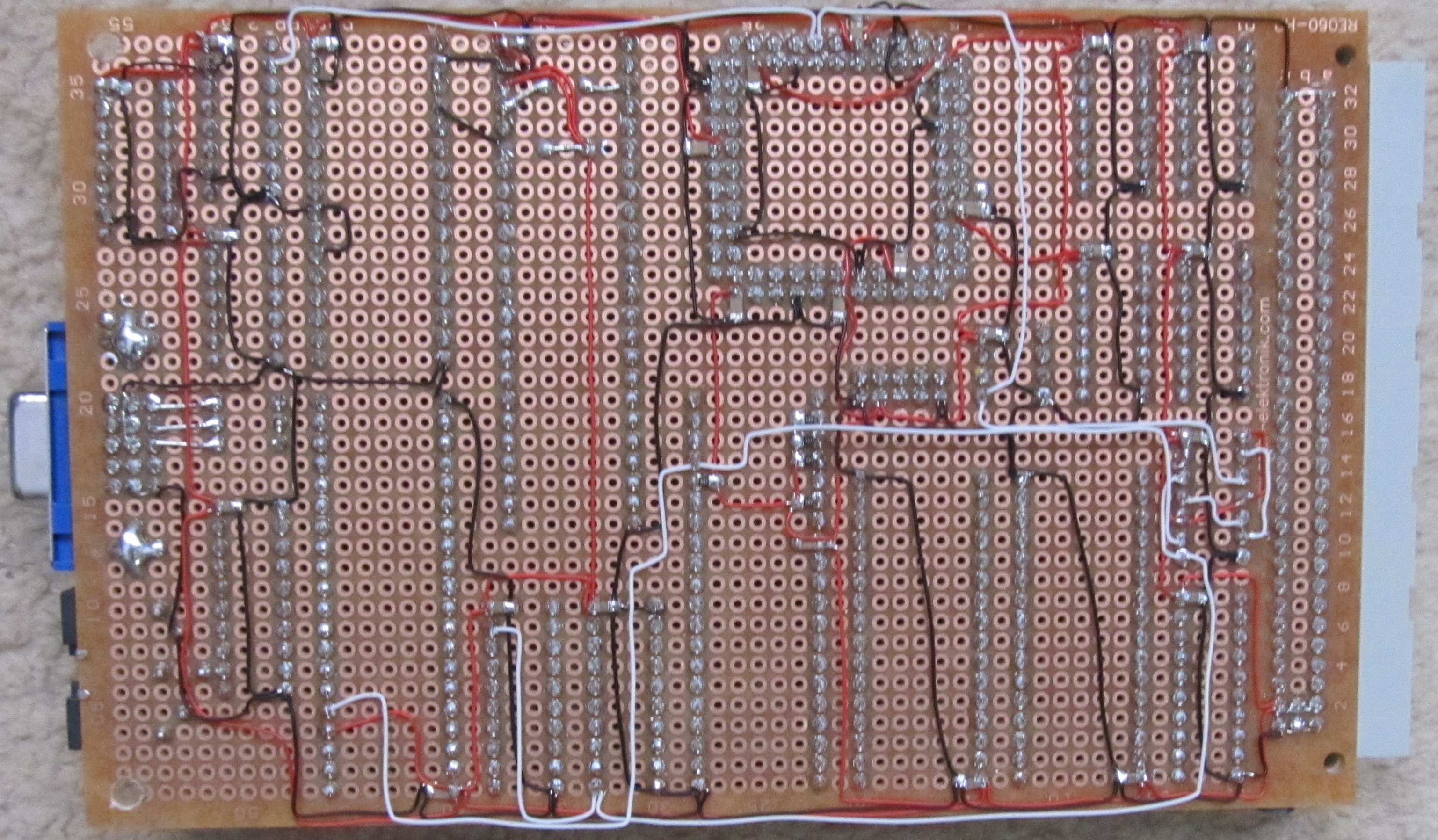
Now for the hard work - wiring the board !
Power, Ground and Clock (white wires) signals have
been connected.
This is actually a
disproportionate amount of work than the number of
wires would suggest. Power and Ground require
multiple terminations, whereas many of the signal
wires are just point-to-point connections. |
 |
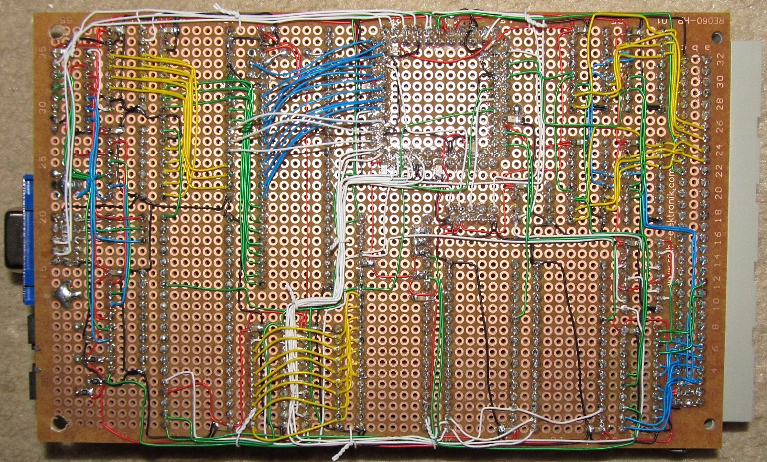
Now with most of the video signal wiring done . . .
The CPLD will be responsible for generating a 10
or 11 bit video address to the VRAM. (blue wires)
The VRAM data output (green) along with 3 bit row
counter from the CPLD (white) and one bit from the
VIA produces a 12 bit address to the character rom.
The output from the ROM (yellow) goes to the shift
register next door. The colour (RGB coloured) data
comes from an 8 bit latch with 2 bits unused. |
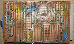 |
The foreground colour data is inverted before
foreground and background data was to the
multiplexer driven by the shift register output.
Inverting the foreground colour from the latch will
ensure a default output of white on black.
In this slide, the majority of the wiring is done,
just the low half of the address bus and the data
bus need to be completed, but as you can see, the
wiring around the CPLD is pretty conjested. |
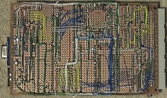 |
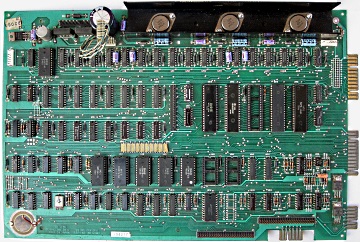
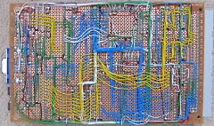
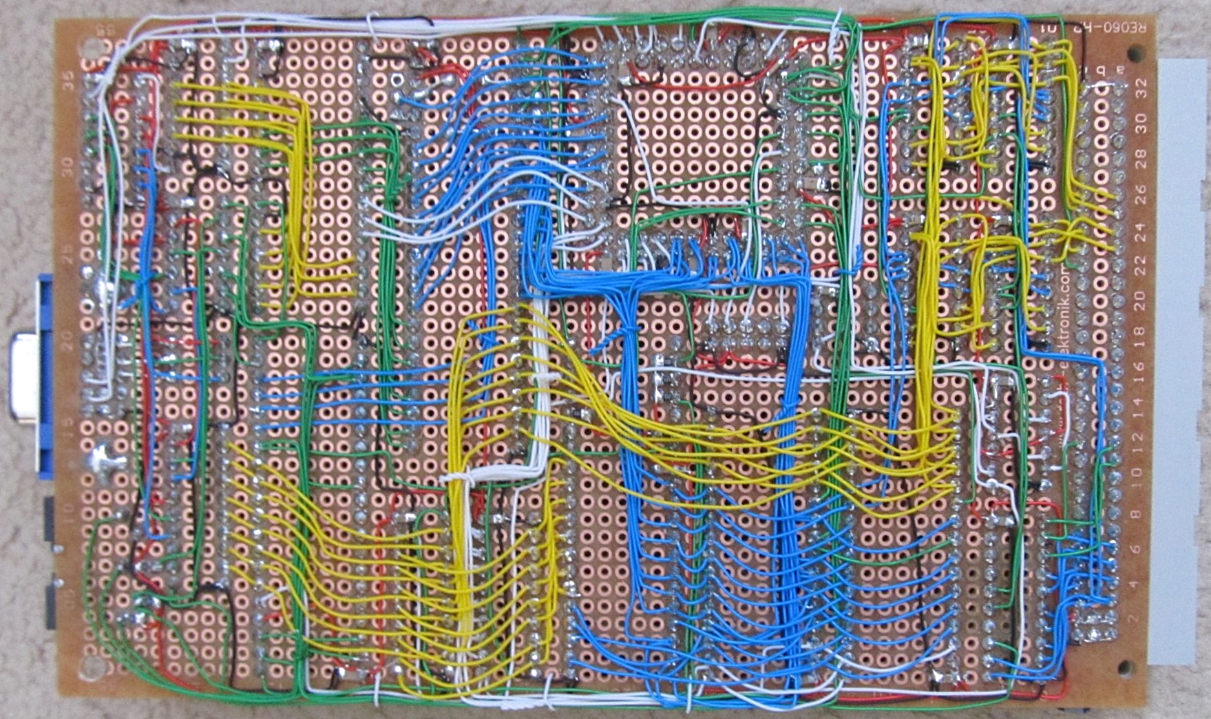
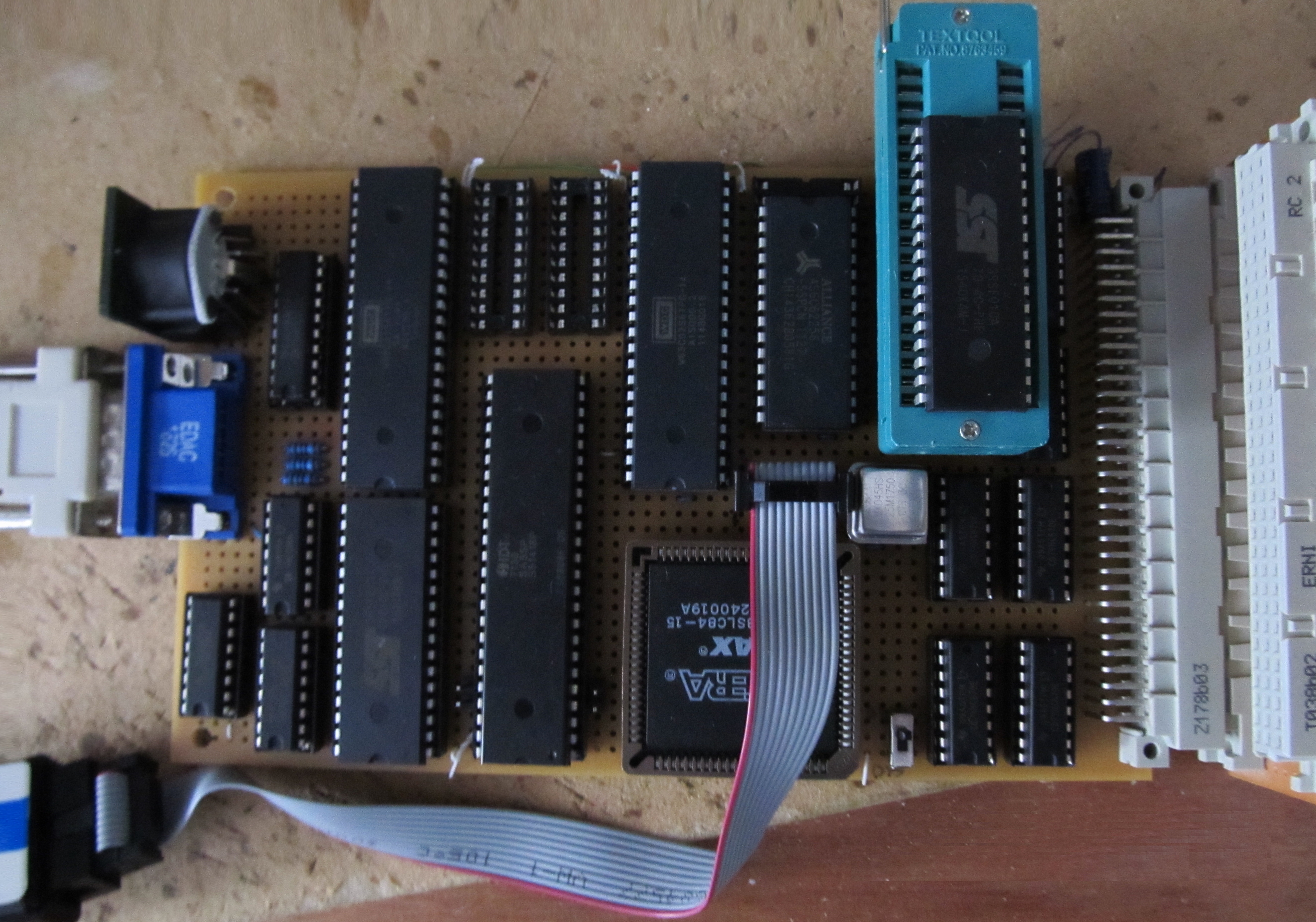
Phew ! - The MemoPET board is now fully wired.
Martin has made a couple of changes to the
design along the way . . . .
The CPLD now
has all 3 clocks fed to it. The shift register isn't
connected directly to the VGA clock any more, that's
connected to a spare CPLD pin. |
 |
That means that, theoretically, the CPLD can
produce a 40 column display using the intermediate
half VGA clock, as well as 80 columns from the
standard clock. The 1/4 speed clock drives the CPU
and VIA at 6.3mhs so the CPLD needs that for the
read/write logic.
Reflecting these changes,
the schematic has been updated |
 |
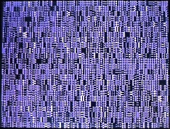
With the wiring completed, here you can see the
first video output.
If you open up the larger
image file, you can see that there are characters
being produced from the Vic-20 character set.
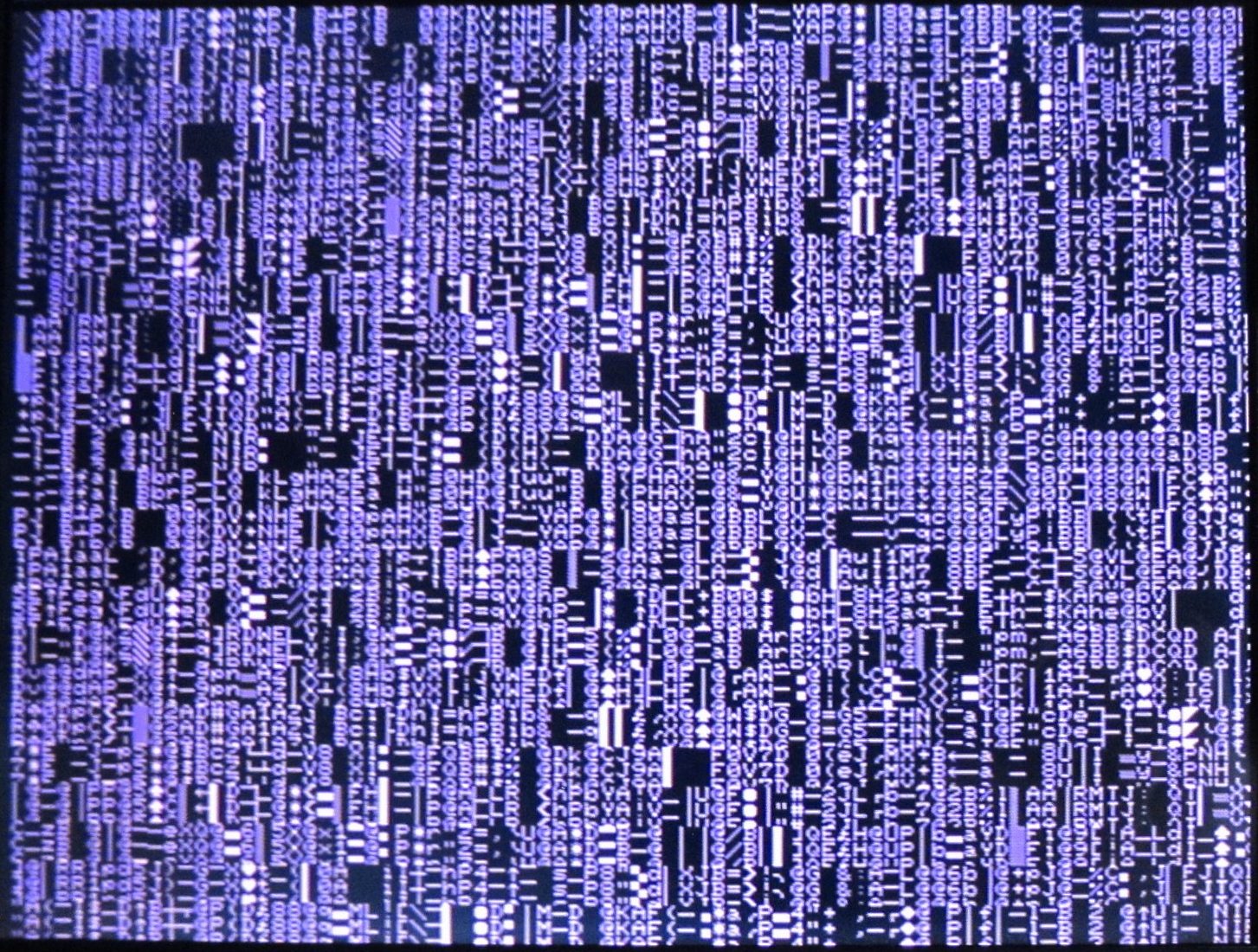
Obviously, there are issues such as the
character colour (which should be white, not violet)
and the matrix size, but this is a great start. |
 |
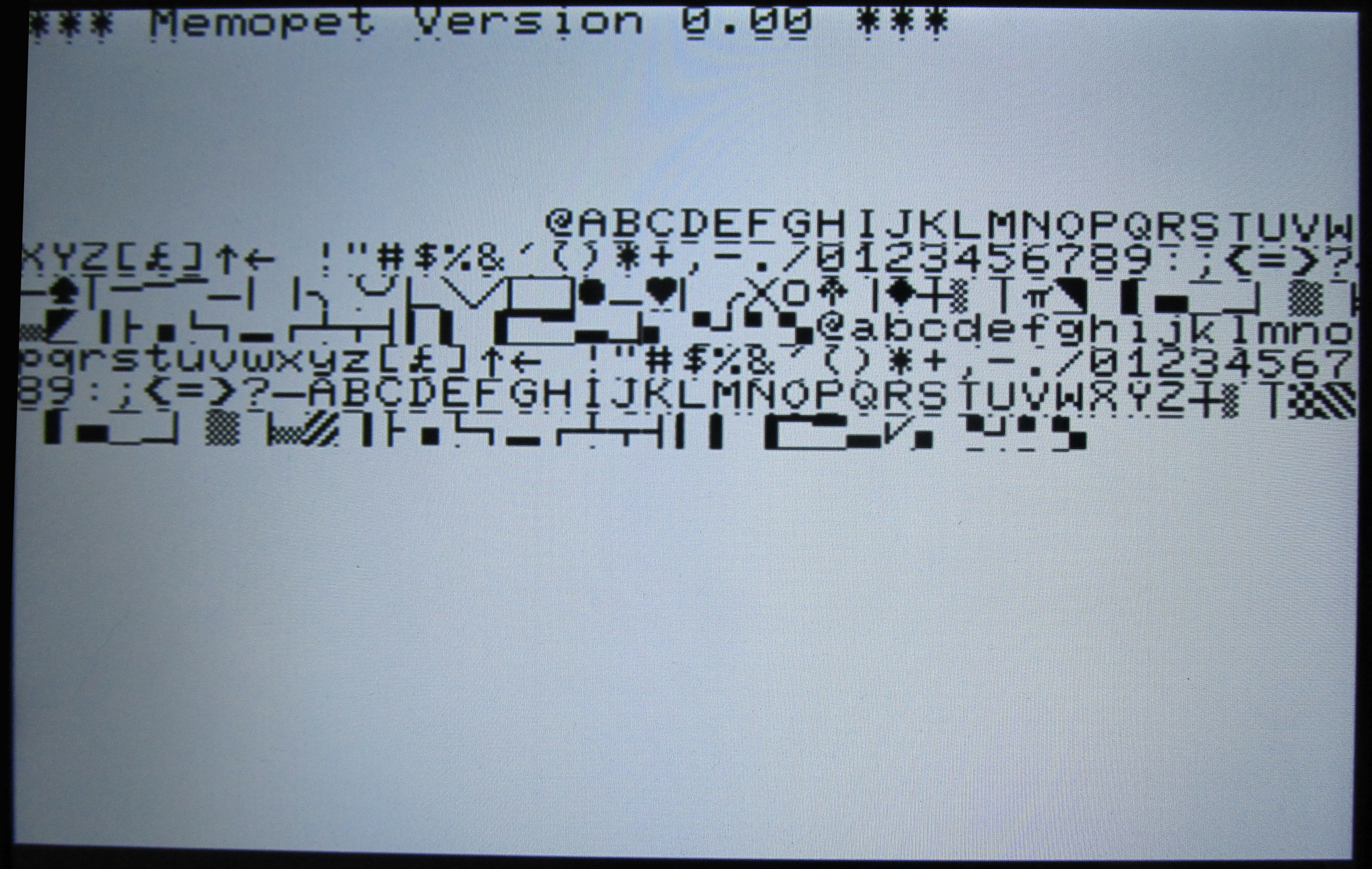
After a little "tweaking" of the software, a more
recognisable PET like display.
The display
is inverted, but that will be resolved by selecting
the other output from the shift register. The
display is currently missing a small portion of the
left hand character, but that will be resolved by
adjusting the video timing slightly. |
 |
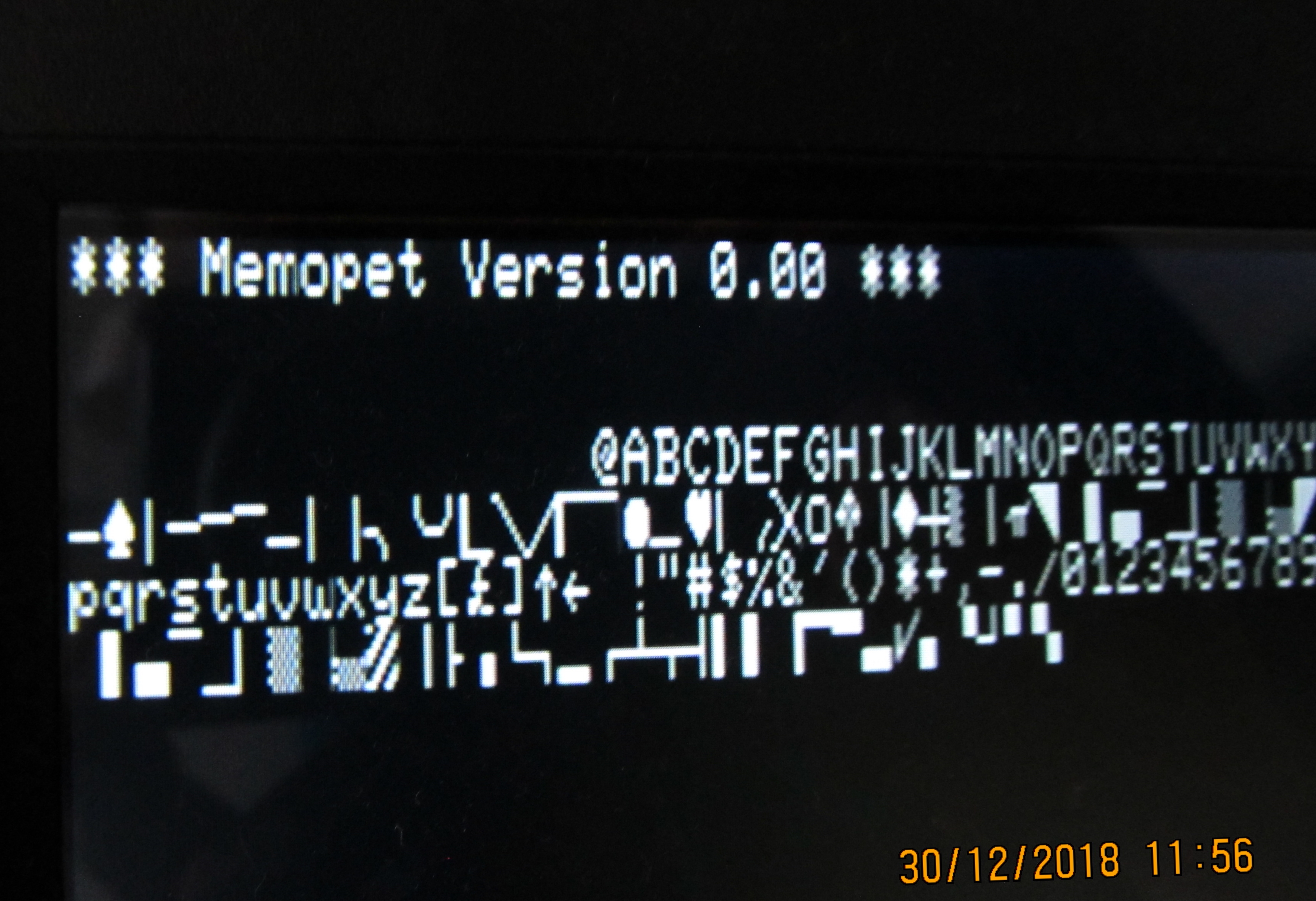
Video inversion fixed and screen alignment almost
resolved.
In the next two images, you can see
that the screen is correctly displaying 40
characters. |
 |
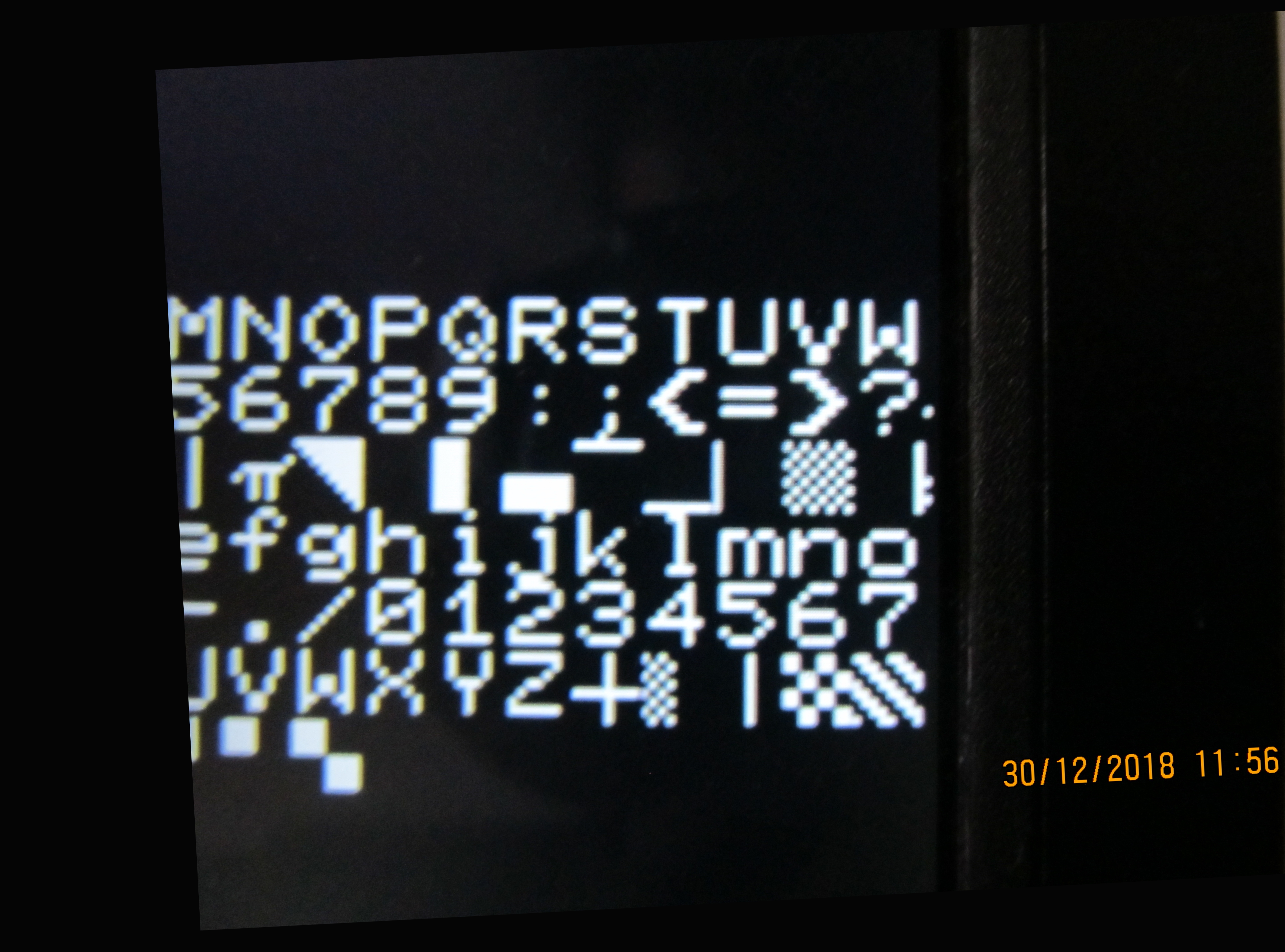
But if you look very closely, you may be able to see
that the first pixel of each character is a little
wider than it should be, while the last pixel is a
little narrower.
This will be fixed by adding
an R-C delay, rather than messing with the CPLD
code. |
 |
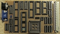
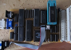
The assembled board, plugged into the
MTXPlus+ backplane.
The two unpopulated
sockets are no longer needed and the ZIF socket is
just installed for ease of testing ROM updates.
Now that the display system is pretty much
working, the next, and bigger, challenge, is to get
the disk I/O interface working. |
 |
|
Updated schematic - open the PDF to for some brief
details of how the board PIA and VIA work in
comparison to a PET or VIC-20. |
 |
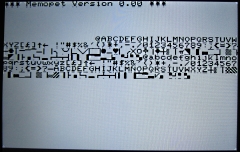
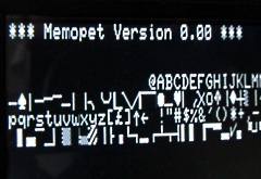
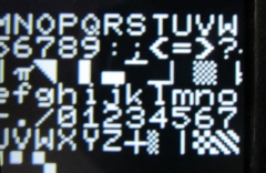
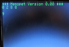
A little taster . . .
The 20k, 40 column PET
ROM image into loaded into the flash in the MemoPET.
Obviously, there's no support for anything other
than the screen memory, but it's a promising start! |
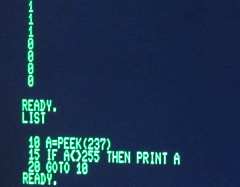
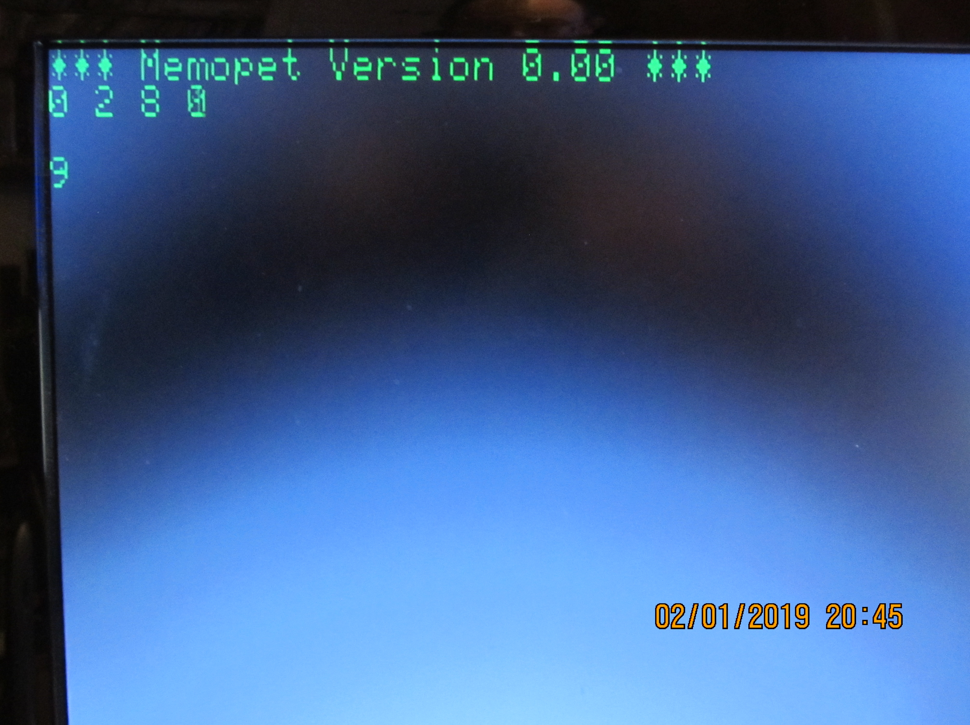
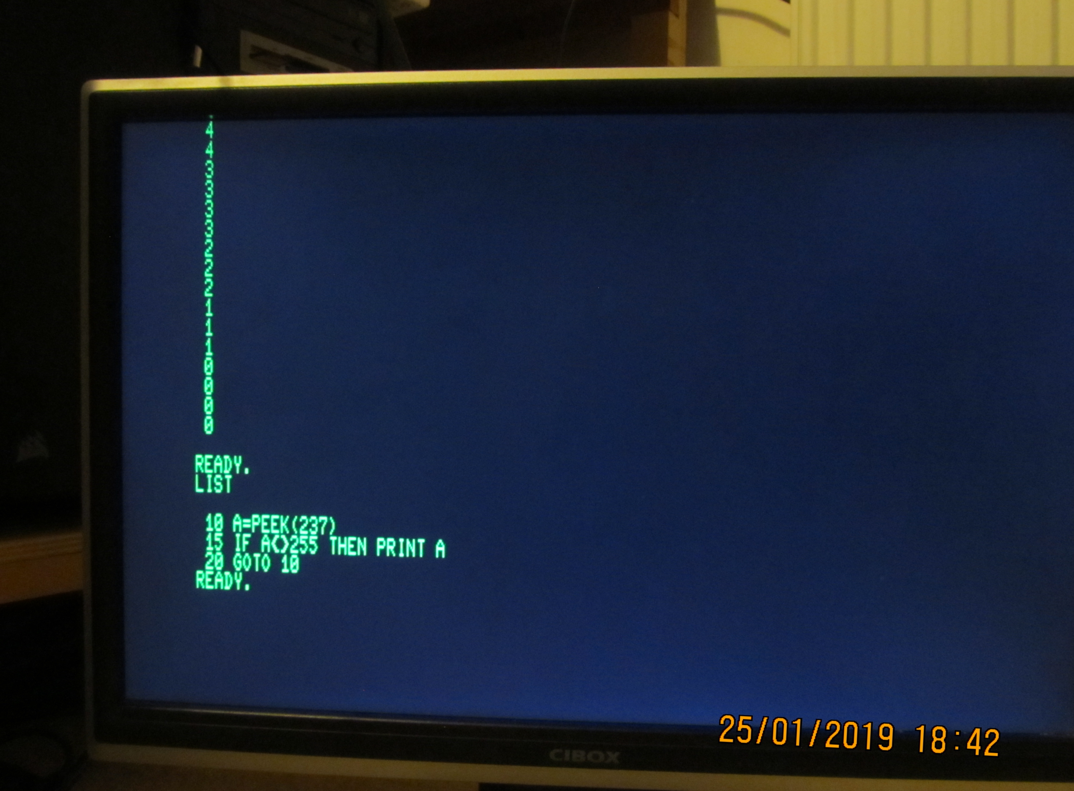
 |
This image shows the PET RAM being written to from
the MTXPlus+. A
BASIC program on the MTXPlus+ side writes data
to a 4 digit counter and triggers an NMI interrupt
on the 6502 side.
The MemoPET output shows
the values of the four digit counter on the second
line and the value of the interrupt counter on the
fourth line. |
 |
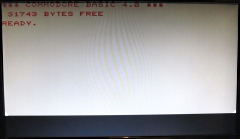
Now looking remarkably "PET like" !
Using a
modified Editor ROM, created with some help from
Steve Gray's PET Editor ROM pages, and adding
elements from the PET BASIC 4 and Kernel ROMs things
are starting to come together nicely.
At this
stage, there were some issues with key-mapping and
keyboard de-bounce, but things are obviously
progressing . . . . |
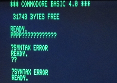 |
Now demonstrating a running Commodore PET BASIC
program.
The program was printing numbers
that were counting down under IRQ control, derived
from the vertical blank interrupt. The program has
been stopped in a similar way that a "real" PET
BASIC program would be stopped with the Run/Stop
Key.
Still to be completed are the I/O
routines that can drive simple sound output and an
emulated disk drive (IEEE-488/IEC) interface like
the PET, or more accurately, the VIC-20. |
 |
|
|
|
|
|
|
|
|
|
Placeholder
|