|
 |
The Memotech MTX Series |
 |
Martin Allcorn's Games ROM
 |
 |
 |
|
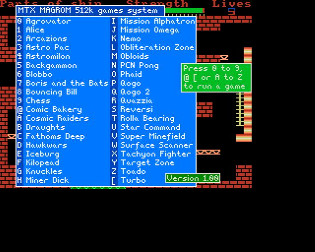
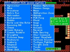
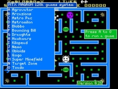
512KB, 38 Game ROM |
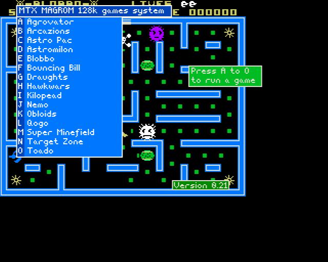
128KB, 15 Game ROM |
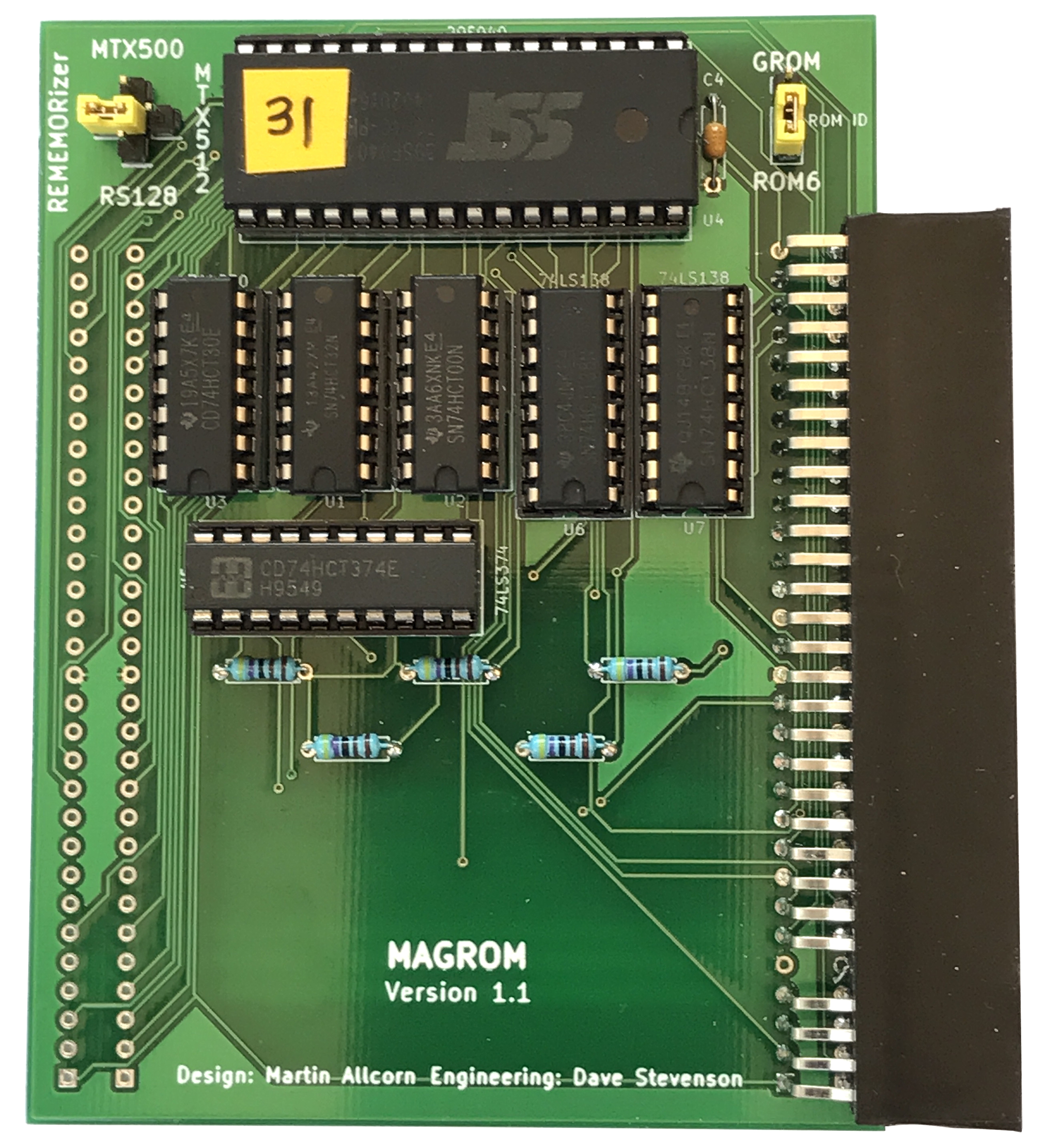
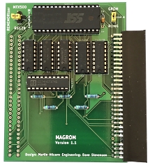
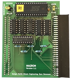
MAGROM - Version 1.1
(Do you want one ?)
Introduction
MAGROM Version 1.1 has two improvements over the
original:
- Support for REMEMOrizer
- Configurable ROM ID selection
And one unintended consequence
The
User's
Manual describes how to install and use MAGROM Version 1.1
REMEMOrizer
"Out of the box", MAGROM Version 1 wasn't
compatible with Andy Key's
REMEMOrizer due to the way that REMEMOrizer makes 384K of
RAM available in ROM mode, more than a standard MTX was able
to provide and more than the original MAGROM design was able
to cope
with. This was particularly problematic for users who had
removed the original OS ROM to allow REMEMOrizer to provide
Andy's enhanced OS ROM as the original ROM would have needed to be
replaced to allow MAGROM to work.
It was possible to patch the MAGROM board to allow it to be
used with REMEMOrizer, these patches have now been incorporated
into the standard design.
Errata: After almost 20 Version 1.1 boards
had shipped, I discovered that I had reversed the REMEMORizer
and RS128 jumper labels. This cosmetic issue will be corrected
when/if another run of PCBs is manufactured.
ROM ID Selection
The MTX computer was designed to support plug-in Games ROMs that used
the interface GROM signal to enable Games ROMs with an ID of 7.
MAGROM was designed to use the same ROM ID to provide multi-game
support. However, some MTX owners with foreign language MTXs were
unable to use MAGROM due to the way that Memotech implemented
foreign language support on some, but not all, regionalised
MTXs.
The MAGROM design has been modified to allow the user to
select either ROM 7 or ROM 6 as required.
How it Works
The HC32 chip, U1 on the KiCad schematic, is used to combine
the Z80’s active low write (WR)
and I/O request (IORQ)
signals into a combined (active low) IO write signal and also
read (RD)
and memory request (MREQ)
into a single memory read. The other 2 gates are unused, and
their inputs tied to 0v.
On start up, the MTX OS scans the paged ROM space at 02000h
looking for the auto start signature, if it’s found, then the
ROM is entered by a jump to 02010h. The controlling ROM
therefore has to be paged in for the address block 02000h to
03fffh.
The easiest way to do this is use the
GROM
signal on the edge connector which goes low when ROM page 7 is
accessed and was originally intended for use by games ROM
expansion packs. MAGROM V1.0 operates using this signal.
However, Memotech re-purposed the signal to activate the
piggyback ROM in some of the non English language MTX systems.
This unfortunately prevents MAGROM 1.0 working.
Version 1.1 of the board is designed to work around this by
allowing the control software to appear in ROM page 6 instead.
This is done by the extra HCT138 chip, U7. The 3 address
selectors, on pins 1-3, are fed with R0-R2 from the edge
connector, and the chip enables are connected A13 to the active
high pin 6, while A14 and A15 go to the active low enables. This
ensures the output is low only in the correct memory region. Any
of the ROM pages from 2-7 could be used this way, but 6 was
chosen so as not to clash with the maximum amount of other MTX
hardware.
The Y6 output is therefore fed into the ROM6/ROM7 jumper.
GROM
is fed into the ROM7 side. In systems without the language ROM
U7 can be left off entirely and the jumper set to use ROM7 as in
version 1.0.
In addition to providing the control software the ROM also
has to hold the game images. This is to save board space and
cost, as otherwise space would have to be found for a 28pin 8k
EPROM as well as the 512k data ROM. It does reduce the space
available for games by 8k but the remaining 504k turned out to
be more than adequate.
The MTX’s memory map, changes between the various models, but
if you believe
Andy’s Memu pages
and the original MTX manual, they all have one thing in common.
The final page of RAM will have a half page that runs from
08000h to 0BFFFh. (If you have a look at both the old manual on
page 246, and the new one on page 244 you’ll see they disagree
about the half page’s position for the 128k expansion.)
For the MTX500 it’s page 0, for the MTX512 it’s page 1, and
the RS128 it’s page 3. Andy’s REMEMOrizor expansion provides a
LOT of extra memory for basic, though it too has a half page,
but on page 11. The version 1.0 MAGROM needed some “yellow wire”
mods in order to work with REMEMOrizor. V1.1 effectively has
those mods built in.
The data part of the ROM is paged in in the RAM memory map
between 04000h and 7FFFh, so as not to cause a bus clash, the
page used has to be adjusted manually depending on the model.
The software expects there to be RAM above the ROM which
prevents the board from using page 11 on all systems. The HC138
U6 has A14 connected to the active high enable, and A15 and P2
connected to the active low, P0, P1 and P3 are connected to the
address selectors. This makes it possible to place the data rom
in any of the pages 0-3 or 8-11.
The + shape jumper on the board replaces the T jumper on
version 1.0. It is used to select which one of the 4 outputs Y0,
Y1, Y3 or Y7 (for page 11) is treated as the second ROM select
signal. Whichever ROM select is used, it’s connected to one of
the NAND gates on the HCT00, U2, along with the ROM 6 or ROM 7
signal from the other jumper. That is then run through a 2nd
NAND gate configured as an inverter to form the combined ROM
select signal.
In order to prevent any part of the rom paging in while
the system is running in an all ram configuration, the RELCPMH
signal from the page port is combined with the rom select in U1
the quad 2 input OR, if the ROMs are supposed to be paged out
RELCPMH is high and so prevents the ROM select from going low.
The data ROM has to be accessed through a 16k window in
memory, so needs to use a paging system I’ve used an 8 input
NAND with A2 inverted, U3 to detect 0FBh on the lower part of
the address bus. The port address is combined with the IO write
signal form U1 so that the paging register is only selected by
an IO access and not a memory access that happens to have &FB in
the lower part of the address.
Using one ROM for 2 jobs adds in a complication, when
accessing the rom to run the control program, the upper address
bits all need to be zero to point to the correct segment.
However, in data mode the outputs need to be active as all of
the ROM needs to be accessible.
Using a 3 state octal flip-flop as the paging register, with
pull down resistors solves this. A spare gate on the HCT00 (U2)
inverts A14 to provide the active low enable on the HCT374 when
the address is in the data ROM area, but also disables the
outputs then the control part of the ROM is accessed and allow
the resistors to set the upper part of the ROM’s address bus
low.
All the games chosen were written to run on the MTX500 so the
presence of ROM in the memory map doesn’t cause any issues, as
that area’s is empty on the 32k system.
An Unintended Twist
Otherwise known as a mistake!
The layout for the original MAGROM PCB was done using an
earlier release of KiCAD, by the time had I revised the layout
for Version 1.1, I had upgraded to a later version of KiCAD. The
upgrade "broke" some of my KiCAD footprints and I to redo them,
one of the affected components was my MTX Edge Connector
footprint. Unfortunately, when I added the new footprints back
to the layout, I managed to mess up the orientation of J0, the
internal MTX edge connector. This should have been the mirror
image of J10, the external connector, but I forgot to "flip" it.
This means that the left hand side edge connector is unusable on
the V1.1 PCB.
This error will be connected if I ever get another run
of MAGROM boards done, but this is likely to be some way off, if
it ever happens at all. As I was (overly) confident that the
Version 1.1 PCBs would be fine, I ordered up a double batch on
the basis that this was very likely to be a last time buy.
The good news is that this is only a minor issue, the board
can still be mounted either internally or externally, but the
choice of which has to be made when the board is assembled - it
is no longer possible to swap it between internal and external
as the design was meant to accommodate.
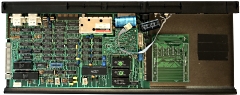
When assembled for external mounting, the edge connector is
fitted under the board, with the component side of the PCB
facing upwards as was the case with the original PCB.
When
assembled for internal mounting, the edge connector is
fitted on the top side of the board.
There is
a slight cost benefit for buyers though, on the original
version, all of the boards were assembled with the
external connector fitted as standard and users opting
for the internal version had to pay for the second
connector to be fitted.
Since the internal fit of
Version 1.1 doesn't use an additional
connector, the prices for the external and internal
versions will be the same. |
 |
| The
PCB must be inverted, i.e., with the component side
facing downwards to install the PCB internally. |
 |
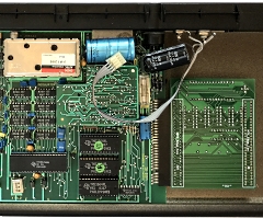
Close up of
the Version 1.1 PCB installed internally.
The
only real downside of having the board upside down is
that it needs to be removed to reset the jumpers, but
that is only likely to be a one-time operation unless
the machine's RAM size was changed or a REMEMOrizer was
fitted after MAGROM was installed. |
 |
|