|
 |
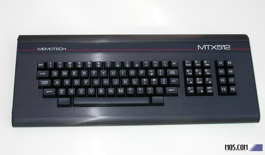
The Memotech MTX Series |
 |
Memotech Technical Information
This page contains some detailed technical data on the
Memotech MTX interfaces, I have not verified it's accuracy and
take no responsibility if you use any of this data and your MTX
explodes, your cat dies or the banking system collapses (as if
!) as a result, or not, of using anything you find on this page.
03/10/2012 Updated - see footnote
Memotech MTX500 and MTX512 computers were very much aimed at
the same market as the BBC model B machine and, accordingly,
they have very impressive input and output capabilities.
It would be an exaggeration to say that the Memotech machines
are equal to the BBC model B in terms of input/output capability
(there is no analogue port on the MTX500/512 for example), but
there is a useful range of ports fitted as standard, plus an
expansion bus which makes available the full data, address, and
control busses.
An attractive feature of these machines from the add-on
enthusiasts point of view, and one which they have in common
with the BBC machines is the inclusion of a built-in assembler
which can make software writing very much easier when dealing
with specialised hardware add-ons which must operate at high
speed
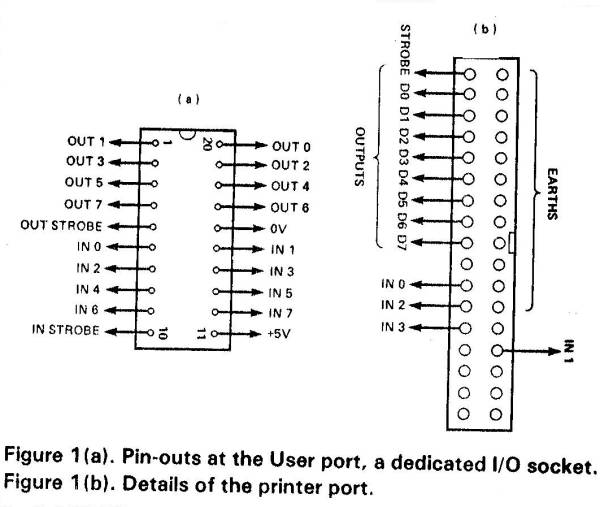
User Port
A user port enables many useful add-on circuits to be very
easily interfaced to a computer, and a port of this type is
available in the Memotech computers. It is unusual in more than
one respect.
The most obvious difference between the Memotech user port
and those fitted to computers such as the BBC model B and VIC
20, is that the Memotech port is not accessible without opening
up the machine (which involves the removal of six screws using a
small Allen key). The connector for this port is a good quality
20-pin, DIL IC socket which is mounted on the printed circuit
board, and there is a gap at the rear of the computer to enable
a ribbon cable to run through to the outside world.
The choice of a 20-pin DIL IC socket is not a very convenient
one for the home-constructor in that 20-pin DIL header plugs do
not seem to be available (although this situation could well
change). Of course, if it is only necessary to make connections
to some of the terminals a 14 or 16-pin plug will probably
suffice. Otherwise it is a matter of cutting down 14-way plugs
to 10 ways each, and using these to make the connections to the
port. For anyone likely to use this with port with a number of
add-ons it would be advisable to make up a lead to take the
connections to a more convenient rope of socket (such as a
20-Way IDC socket) situated on the exterior of the case where it
will be more accessible.
Another unusual aspect of the user port is that it provides
an 8-bit input port and a separate 8-bit output port.
On the face of it this may seem to be more useful than the
more normal arrangement where eight lines are provided (with
each one being programmable as an input or an output plus two
handshake lines. However in practice this is not necessarily the
case.
Many applications require eight input or eight output lines,
plus a handshake input or a handshake output, or both. In other
words quite often nine inputs or nine outputs will be needed and
these are not available on the Memotech user port.
On the other hand, where handshaking is not required, the
ability to use up to eight inputs and eight outputs
simultaneously obviously gives greater potential than the
standard user port arrangement. Figure 1(a) here shows
connection details for the user port. The eight inputs are
provided by a 74LS373 quad transparent latch, and this port is
therefore TTL compatible.
The strobe terminals do not, as one might expect, connect to
the outputs of the address decoder circuit which provides the
chip enable signals for the user port devices.
The input strobe can be used in applications where the input
data will only be present momentarily, and a high strobe pulse
applied to this input will latch data into the port.
The output port is provided by a 74LS374 three state octal
D-type flip/flop, and it therefore provides TTL compatible
output signals.
This port normally has its outputs in the high impedance
state, and the output strobe terminal must be taken low to
enable data to be taken from the port. The output strobe
terminal will simply be tied to earth in the majority of
applications. The maximum output current that can be drawn from
the 5 volt output of the port is stated as being a rather
miserly 20 milliamps, but it is presumably possible to take more
than this if no expansion boards are fitted to the computer
Basic Control
Communication with the port from BASIC is possible using the
OUT instruction and the INP function (not the more common IN
function).
If we take the OUT instruction first, this is followed by two
numbers; the port address and the number to be written to that
port. The address and the number written are both integers from
0 to 255, and the user port is at address 7. The number written
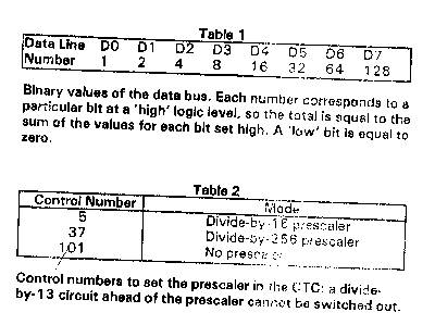
to the port controls the output lines in standard binary
fashion. The table simply shows the number required to set each
line in the high state, and in order to set several lines high
it %s merely necessary to use the sum of the relevant numbers.
For/example, to set D0 to D3 high the command OUT 7,15 would be
used (1+2+4+8=15).
The INP function operates in the reverse fashion, and if D0
to D3 of the input port are high, while D4 to D7 are low, the
command PRINT INP(7) would return a value of 15. In other words
the table shows the number that each input line contributes to
the returned number if it is set high (zero is always
contributed by a line that is low).
The MTX500/512 computers have a BASIC AND function, but this
can not be used as a logical operator to mask unwanted bits when
reading an input port. The way in which an AND masking system
operates is very straightforward; it is just a matter of ANDing
the number returned from the port with the number that would be
produced by the bits that are of interest if they were all in
the high state. For instance, if lines 4, 5, 6, and 7 are the
only ones we wish to read, when set high these return a total
value of 240 (16+ 32+ 64+ 128= 240). By ANDing the number
returned from the port with 240, only the four most significant
bits (4 to 7) can contribute to the returned number, and the
unwanted bits (0 to 3) are effectively set at zero.
Although the MTX500/512 computers can not provide this type
of AND function from BASIC, it is in the repertoire the Z80A
microprocessor use in these machines, and it can be achieved
with the aid of a short assembly language routine. A suitable
routine would be…
10 CODE
8007 LD A,0
8009 LDB,A
800A IN A,(7)
800C AND 170
800E LD C,A
800F RET
20 PRINT
USR(32775)
Refer to the MTX500/512 manual for details of how to enter an
assembly language routine,
Line 10 provides the assembled machine code while line 20
prints the returned value on the screen using the USR function.
Although the address at line 20 (32775) does not seem to be the
same as the start address of the machine code routine (8007),
this is simply because the former is in decimal and the latter
is in hexadecimal.
The number after the AND instruction (170) is given only as
an example, and this should be replaced by the appropriate
masking number.
Printer Port
A parallel printer port is a standard interface of the
MTX500/512 machines, and this can also be used as an
input/output port for user add-ons.
In fact it is probably better to use this port rather than
the user port in applications where it provides sufficient
input/output lines, since it is far more accessible. It is one
of the ports on the rear panel of the machine, and it uses a
standard 34-way IDC connector.
Expansion Bus
Details of the expansion bus are provided in Figure 2. This
is the bus which is externally accessible. The internal bus at
the opposite end of the printed circuit board is the same, but
is a "mirror image" of Figure 2.
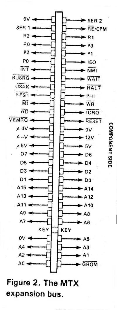
Connection to the bus is via a 2-by-30 way 0.1 inch pitch
edge connector. There is provision for a polarising key at
position 5 of the connector, but as yet 2-by-30 way connectors
fitted with a suitable key do not seem to be available.
An ordinary 2-by-30 way type can be used, with either a key
being fitted by the user or due care taken not to fit the
connector round the wrong way!
What is probably a better solution is to use a Spectrum type
2-by-28 way connector which has a suitable polarising key.
However, this is only possible if no connections to the four
terminals at the left-hand end of the connector are required
(which will usually be the case).
For those who are unfamiliar with the Z80 method of
interfacing, it should perhaps be explained that input and
output devices have a separate map; they are not memory mapped.
Only the eight least significant address lines (A0 to A7) are
used for input/output devices, giving a total of 256 possible
addresses from 0 to 255. Most of these are used by internal
circuits or are reserved for Memotech expansion boards, although
it is obviously possible to use addresses reserved for the
latter if you do not intend to use any of these expansions.
There is some free address range for user add-ons, and the
relevant address range is from 16 to 30 inclusive. This enables
some fifteen input devices and fifteen output circuits to be
added, which is likely to be more than adequate in practice.
Apart from decoding the eight address lines, the (Active
High) MI, IORQ , RD, and WR lines must also be decoded.
IORQ goes low when an input/output device (rather than a
memory circuit) is being addressed, and MI goes low together
with IOI3 when an interrupt is being acknowledged by the
microprocessor. The address decoder mast therefore only be
activated when IORQ is low but MI is high.
RD goes low when the microprocessor is reading an input or
memory device, and goes low when a write operation is in
progress. The way in which these are decoded depends on whether
the decoder is for an input circuit or an output type.
Decoding
Figure 3 shows the circuit diagram of a decoder suitable far
use with MT'X500/512 computers.
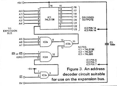
The three address inputs of ICI. (a 74LS1383 3-to-8 line
decoder) are used to decode address lines A0 to A2. The other
inputs are decoded by gates of IC2 and IC3 plus the chip enable
inputs of ICI. This gives eight decided outputs which correspond
to the addresses from 16 to 23.
Either the (Active High) RD or (Active High) WR line is
decoded by the circuit, depending an whether the decoder is to
be used with input or output circuits. The decoded outputs
provide negative chip enable pulses, incidentally.
Note that one section of IC2 and two sections of IC3 are not
used in this circuit, and the unused sections are simply
ignored.
Figure 4 shows the circuit of an 8-bit latching output port
for use with the decoder circuit.
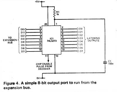
ICI is an octal D-type flip/flop which is used here as an
octal latch with the latching pulse from the decoder being
applied to the clock input.
R1 to C1 provide a negative pulse to the reset input at
switch-on, and this sets all the outputs to the low state
initially.
Figure 5 shows the circuit diagram of an 8-bit input port for
use with the decoder circuit, and this is essentially the same
as the input port of the user port.
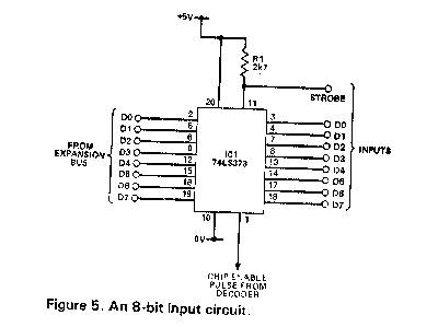
ICI is a 74LS373 octal transparent latch with three state
outputs. The chip enable pulse sets the outputs to the active
state so that they can be read by the microprocessor.
The latches are normally in the transparent state, and data
present at the inputs can therefore be read by the
microprocessor.
However, like the inputs of the user port, a latching action
can be provided by having the strobe input normally low, and
providing a high latching pulse when valid input data is
present. This data can then be read at any time by the
microprocessor.
Counter/Timer
The MTX500/512 computers include a Z80ACTC counter timer
device, which has four 8-bit counter timers. These are used for
the real time clock and to provide the clock signals for the
optional twin RS232C serial interface.
As access to the two outputs used for the serial interface
clock signals is available on the expansion bus (SER1 and SER2),
two channels of the timer counter are available for user
add-ons.
However, this assumes that the RS232C interface is not
fitted, and in any case the two available channels can only be
utilised in a very limited way.
The only mode of operation available is the one where the
timers are used to divide the machine clock frequency to provide
a relatively low frequency clock signal. There are some
applications where this facility could be of great value.
There is built-in software to control the timers, and the
BASIC BAUD instruction can be used to set the output
frequencies.
This only gives a limited range of output frequencies (ten
baud rates are accommodated), although this is ideal for a
home-constructed serial interface of some kind.
Note that the output frequency is sixteen times the selected
baud rate, and the unit is arranged this way simply because most
serial interface devices have a built-in divider circuit and
need a clock at sixteen times the transmitted data rate. Thus,
for example, the command BAUD 0,75 produces an output frequency
of 1.2 kHz on SER 1.
The CTC circuit can be controlled directly by writing data to
output addresses 9 and 10. The clock signal is divided by 13
prior to being fed to the CTC circuit, and it can be further
divided by 16 or 256 using the built-in prescaler.
The main timer circuit then divides the signal by any value
from 1 to 256. SER 1 is effectively at address 9 while SER 2 is
controlled by writing to address 10.
First a control number must be written to set the desired
mode of operation, as detailed in Table 2. Then the number by
which the main timer must divide the signal is written to the
device. For instance:
OUT 9,5
OUT 9,128
…would set the device in the divide by 16 prescaler
mode, with the main timer dividing the signal by 128.
As the clock frequency is 4MHZ, and taking into account the
divide by thirteen circuit ahead of the CTC, this would give an
output frequency of 150.24Hz
A total of 768 frequencies ran be provided, ranging from a
minimum of just under 5Hz to a maximum of a little over 300KHz
One final point regarding the expansion bus is that the "-V"
output is not a -5 volt supply. This is a non-regulated negative
supply which measured up at about -12 volts.
Footnote:
This is one of the articles that I downloaded from the web some
years ago. As it turns out, someone had manually transcribed an
article from Digital and Microelectronics of August/September
1984 by R.A. Penfold, entitled "Interfaces For The Memotech MTX".
Although I did not recognise it at the time, I already had a
copy of this article pulled from the original magazine. You can
read the original article here.
Additional electronics projects for the MTX can be found on the
legacy projects page.
|