|
 |
The Memotech MTX Series
|
 |
MTX Series RAM Selection
/ Decoding - MTX512S2
Disclaimer
This information on this page is based on my limited
understanding of the subject, aided by discussion in the
Facebook MTX500 Group with contributions from the likes of
Tony Brewer and Andy Key - any errors are all mine though - if you spot any, please let
me know.
MTX512S2
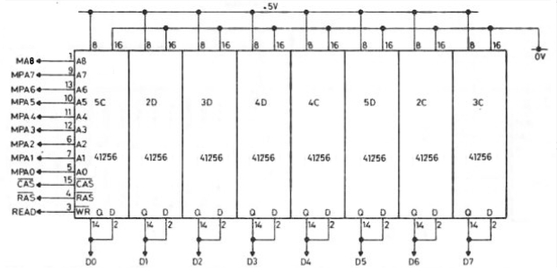
The MTX512S2 modified the computer board to accept 256K x
1 bit DRAM chips.
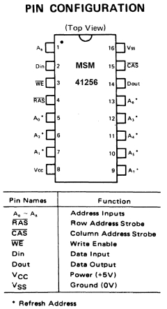
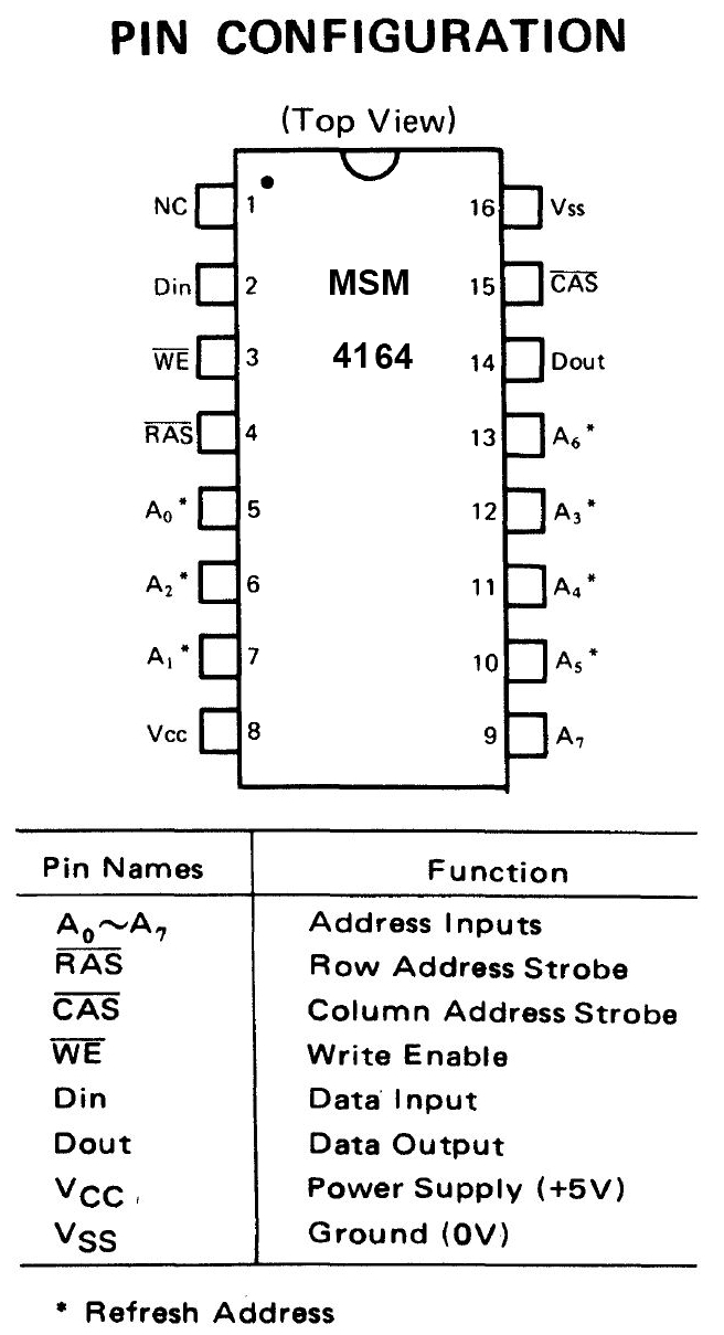
| As these examples of OKI DRAM chips show, a
256K x 1 DRAM uses an additional address pin
than a 64K x 1 does.
Conveniently, Pin 1 on an OKI MSM4164 DRAM
was not used and the additional pin for the A8
address line on a 256K DRAM is also on Pin 1.
In order to support the 256K DRAMs, Memotech
had to wire the A8 address line from Pin 1 of the
8 DRAMs to the PAL.
However, using RAS
only refresh, a 256K DRAM needs 256 refresh cycles - the
Z80 7-bit counter could not have supported this
without an additional modification to increment
the A8 address bit external to the
Z80. |
 |
 |
| However, 256K memories also support the
CAS
before
RAS
refresh technique.
In this method, the refresh counter is internal to the DRAM
and the address bus inputs are not used, i.e., the RAM has
an on-chip refresh capability. The MTX512S2 was modified
to use
CAS
before
RAS
refresh, rather than the RAS
only refresh, of the earlier models.
Memotech had to make a relatively simple wiring
change to the
CAS
timing chain to change the refresh method. By
inspection of the photos of the jumper wires
added to the MTX512S2, Tony Brewer was able to
determine that the only change was the order of
the last two gates in the
CAS
timing chain (click
for a photo of the modifications).
This minor change has no effect on the delays
and the
CAS
signal would lag RAS
by the same time as previously, ~60ms. |
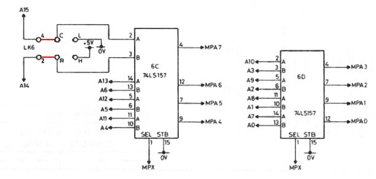
As described on
Andy's hardware web page, and on
the previous page, for the
earlier MTX computers, the A7 input to the DRAMs
is normally multiplexed from A14 and NA15 (where
NA15 is the modified A15 computed by the address
decoder PAL). However, on the MTX512S2, the A7
input to the DRAMs is now simply multiplexed from A14
and A15.

PAL RAM Control and Address Decoding Logic
- MTX500/MTX512/RS128
PAL RAM Control and Address Decoding Logic
- MTX512S2
For the MTX512S2, both links LK6 and LK7
are now redundant. As for the previous computers, LK7 is not used and now not
even referenced in the PAL equations, links LK6-2
and LK6-4
are fixed in the same positions as for the MTX512.
MTX512S2 PAL Modifications
As described by Andy, "What was previously the NA15
output of the PAL now effectively provides A16 and A17 to
the DRAMs [to the RAM A8 address line]. Which to provide depends on the RAS/CAS logic, so
the the I2H4L input is repurposed and feeds
the MPX signal from the RAS/CAS logic"
back into the
PAL.
This leads to
MTX512S2 PAL equations :-
|
MA8 = |
P0 *
MPX
|
where
|
MA8 is the repurposed NA15
pin, and
|
|
+ |
A14 *
A15 |
the
MPX input replaces the previously
redundant,
I2H4L
pin |
|
RAM = |
A14
*
A15
*
MREQ |
|
+ |
RELCPMH
*
P3
* P2
* MREQ
|
|
+ |
RELCPMH
*
P3
* P2
* P1
* P0
*
A14
*
A15 *
MREQ |
|
+ |
RELCPMH
*
P3
* P2
* P1
*
A14
*
A15
* MREQ
|
ROM Based Memory
Map - RELCPMH = 0
As before, when ROMs are enabled,
they are mapped from 0 to 3FFFh. The 8K (2000h bytes)
monitor ROM is always available in area 0 to 1FFFh and
the paged ROMs of 8K (2000h bytes) each are mapped from
2000h to 3FFFh as eight pages 0 to 7 set by R2, R1, R0
in the page port, write only register.
-
Up to 512K of RAM is mapped on 16 pages (0 to F) set
up by P3, P2 ,P1 and P0 in the page port
write only register.
-
The area C000h to FFFFh is a 16K (4000h bytes) block
common to all RAM pages.
-
The 32K (8000h bytes) block from 4000h to BFFFh is
mapped as 16 pages.
-
The first 48K bytes of RAM for an MTX512S2 is mapped from
4000h to FFFFh (page 0).
|
R2, R1, R0 |
0000 to 1FFFh |
2000 to 3FFFh |
4000 to 7FFFh |
8000 to BFFFh |
C000
to FFFFh |
|
|
000 |
(0) |
MONITOR
A
(OS) |
SYS B (BASIC) |
512S2 |
512S2 |
512S2
4000h Bytes
Common
Block
|
0 |
|
001 |
(1) |
SYS C (ASSEM) |
512S2 |
512S2 |
1 |
|
010 |
(2) |
(ROM 2) |
512S2 |
512S2 |
2 |
|
011 |
(3) |
(ROM 3) |
512S2 |
512S2 |
3 |
|
100 |
(4) |
CP/M boot ROM |
512S2 |
512S2 |
4 |
|
101 |
(5) |
SDX ROM |
512S2 |
512S2 |
5 |
|
110 |
(6) |
(ROM 6) |
512S2 |
512S2 |
6 |
|
111 |
(7) |
CARTRIDGE
|
512S2 |
|
7 |
|
This is an idealised view of what the
MTX512S2
memory map should look like,
with 16 x 16KB
pages of RAM.
|
Again, quoting from Andy's page
. . . .
"It might appear [that an
MTX512S2] would have
256KB of RAM. However, from
BASIC
(i.e.: in RELCPMH=0) mode, there
is only 64KB
visible, and from CP/M (RELCPMH=1)
mode,
208KB of RAM is visible. |
|
|
|
8 |
| |
|
9 |
| |
|
A |
| |
|
B |
| |
|
C |
| |
|
D |
| |
|
E |
| |
|
F |
RAM Based Memory Map - RELCPMH = 1
Again, all ROMs are switched out in this mode
and up to 16 pages of 48K (C000h bytes) are mapped from
0 to BFFFh. These pages are set by P3, P2, P1 and P0 in
the page port write only register. In the
area C000h to FFFFh is a 16K block (4000h bytes) of RAM
common to all pages. Again, the table shows and
idealised view of the RAM, with all 256KB visible to
CP/M, as Andy notes, in reality, only 208KB is visible.
|
0000 to 3FFFh |
4000 to 7FFFh |
8000 to BFFFh |
C000
to FFFFh |
P3, P2, P1, P0 |
| 512S2 |
512S2 |
512S2
|
512S2
4000h Bytes
Common
Block
|
0000 |
(0) |
| 512S2 |
512S2 |
512S2 |
0001 |
(1) |
| 512S2 |
512S2 |
512S2 |
0010 |
(2) |
| 512S2 |
512S2 |
512S2 |
0011 |
(3) |
| 512S2 |
512S2 |
512S2 |
0100 |
(4) |
| |
|
|
0101 |
(5) |
| |
|
|
0110 |
(6) |
| |
|
|
0111 |
(7) |
| |
|
|
1000 |
(8) |
| |
|
|
1001 |
(9) |
| |
|
|
1010 |
(A) |
| |
|
|
1011 |
(B) |
|
|
|
|
1100 |
(C) |
| |
|
|
1101 |
(D) |
| |
|
|
1110 |
(E) |
| |
|
|
1111 |
(F) |
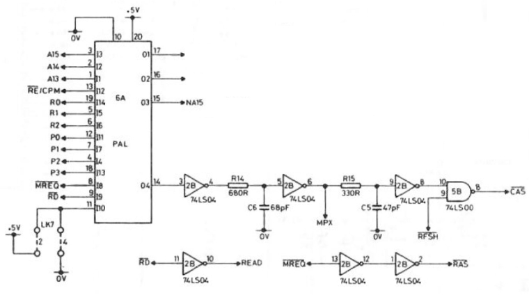
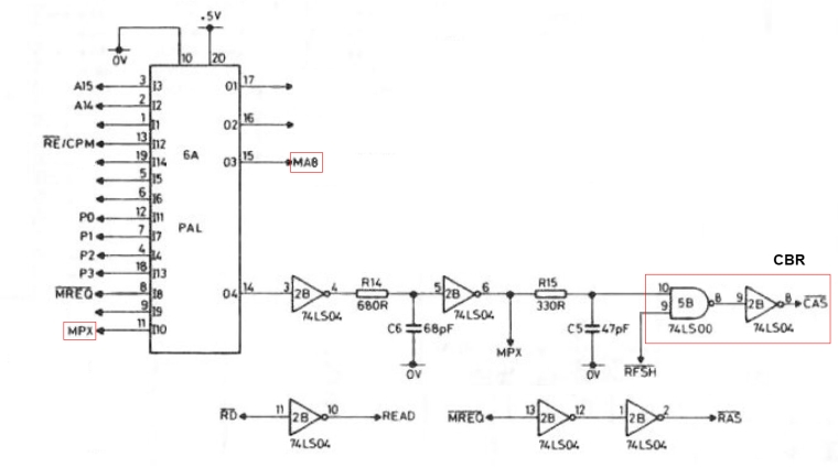
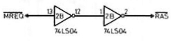
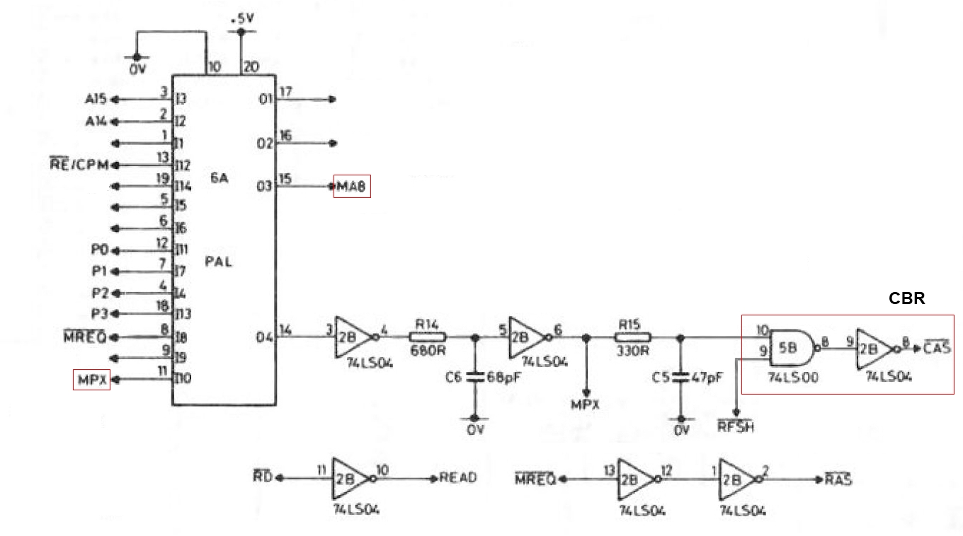
Discrete RAM Control Logic
(MTX512S2)
RAS
Control
The Row Address Strobe (RAS)
is controlled out-with the PAL, and is unchanged from the
earlier models, as shown :-
The circuit diagram shows that the
RAS signal is strobed on every
MREQ high to low transition, i.e., for every Read,
Write or Refresh. In the quiescent state, the
RAM
signal, PAL output O4,
is high, having been inverted twice, the
MPX signal will also be high and the74LS157
data selectors will have their "B" inputs
selected, i.e., A0, A1,
A2, A3, A4, A5,
A6 and A14. When
RAS
is strobed, the data on the address bus lines is passed to
the RAM and forms the row address of the target memory cell.
CAS
Control
The CAS
signal is controlled by the PAL (see above), which sets
Pin 14 low when a memory request is made of the RAM on the
MTX computer board.
As noted above, earlier models of the MTX computer used
RAS
only refresh to control refresh of the DRAM (as
described in detail on the previous
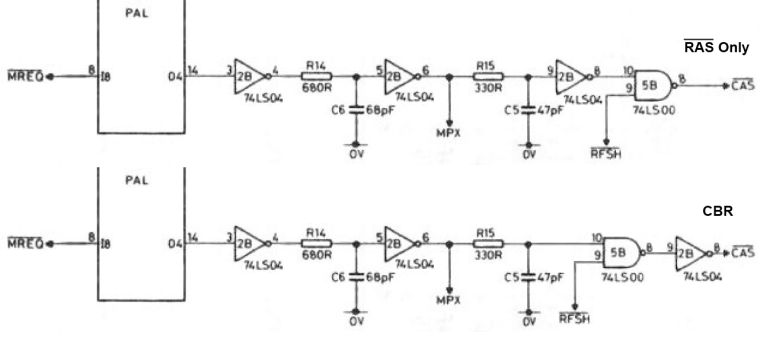
page) and the timing chain circuit marked "RAS
Only" in the diagram, to sequence the CAS
signal.
For a memory read or write operation, after a time delay set
by the values of the R(14)/C(6) network and the inherent
logic gate delays, the MPX signal switches the
74LS157 data selectors to put the data from the remaining
address bus lines, i.e., A7, A8,
A9, A10, A11, A12,
A3 and A15, onto the DRAM
address lines. After a further short delay, set by the
values of the R(15)/C(5) network, the
CAS
signal strobes the data into the DRAM address inputs,
forming the column address of the target memory cell.
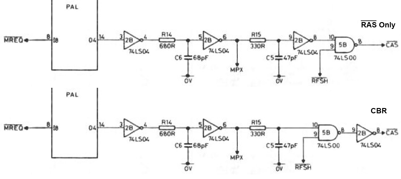
Refresh Control (With thanks to Tony
for helping me understand this bit!)
The
Z80 Databook describes how the refresh signal is
sequenced during an M1 (opcode fetch) cycle. "Clock
state T3 and T4 of a fetch cycle are used to refresh
dynamic memories. During T3 and
T4, the lower seven bits of the address bus contain a
memory refresh address and the RFSH signal becomes
active [low] indicating that a refresh read of all dynamic
memories must be accomplished, during an M1 (opcode
fetch) cycle".
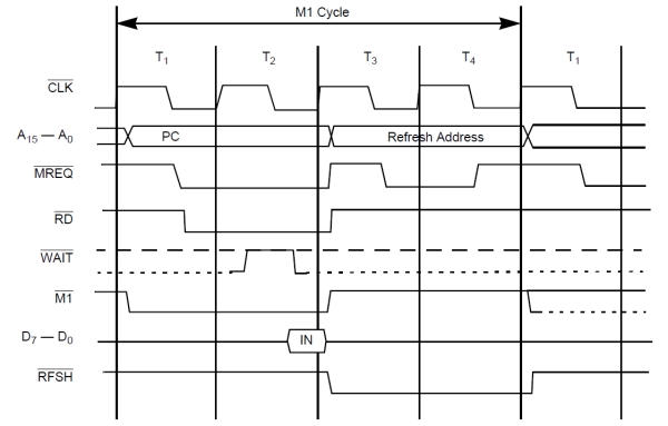
As described
previously, the Z80 R register is
limited to 7 bits and can only directly support 128
refresh cycles. However, as noted above, the 256K x 1 DRAMs in the
MTX512S2 require 256 refresh cycles, the simplest method
of achieving this was for Memotech to use the
CAS
before
RAS
refresh method and have the RAM control refresh
internally. In support of this, the CAS timing chain had
to be modified as shown in the circuit
diagram labelled "CBR".
|
The
M1 Cycle timing diagram shows the
clock periods, referred to as T
(time) cycles.
For
the MTX computer, the clock frequency is 4MHz,
leading to a T period of 1 /
4,000,000, i.e., 250ns.
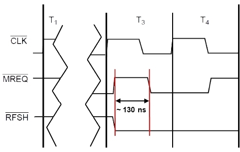
As the close up shows, in the T3 cycle,
the RFSH
signal goes low a relatively long time before
MREQ
- estimated to be of the order of 130ns.
The logic diagrams show that the
RFSH
input is very close to the end of the timing chain, very
close to the
CAS
line output. |
 |
The circuit diagrams show that for the MTX512, the
RFSH
to
CAS
delay is only one gate and in the Series 2, is only two
gates, leading very short delays of ~10 or ~20ns
respectively. In both cases, the
MREQ
to
RAS delay
is two gates (~20 ns). Since the
RFSH
signal is very close to the end of the chain, the
preceding RC delays are not relevant to the refresh
process. During a refresh cycle, since the
RFSH
signal goes low a relatively long time before
MREQ,
CAS
is forced either high (MTX512) or
low (Series 2) before
RAS goes
low.
In summary, the
RFSH input to the NAND forces
CAS
either high during MTX refreshes (RAS-only
refresh) or low during Series 2 refreshes (CAS-before-RAS).
MTX500/512/RS128 <
Previous
Page Goto
Next
Page >
|


