|
 |
The Memotech MTX Series
|
 |
MTX Series Memory Control
Overview
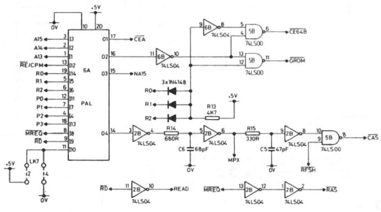
The circuit diagram shows the original memory control logic for
the MTX 500/512/RS128 computers (changes were made for the
MTX512S2), specifically, the 4000-04 computer board. The
diagram is extracted from the
Phoenix MTX
Operators Manual and is the same as that shown in the
Memotech
MTX500/512 Service Manual, it has been corrected to show
that the chip in board position 2B is a 74LS04 (Hex Inverters),
rather than the 74LS14 (Hex
Schmitt Trigger Inverters)
shown in the manuals.
A Programmable Array Logic (PAL)
chip enables custom logic to be programmed into a single
chip, rather than using discrete logic chips. Memotech used
PAL14L4s to control certain memory operations and address
decoding for different
models of MTX computer having differing RAM and ROM
configurations. (Further details of Memotech's use of PAL
chips can be found on my
PAL
Reader page.)
The Service Manual describes the purpose of
the computer board links associated with the different RAM
options.
Link LK7 was intended to identify the installed RAM as either 32kbytes (Link 7,
position 2 for +5v) or 64kbytes (Link 7, position 4 for 0v).
In the PAL equations documented in the Phoenix manual, this
input is referred to as I2H4L (2High
/ 5v, 4Low / 0v). (This input is likely
redundant - as described here.)
Link LK6 is used to select which half of
faulty 64KB RAM chips had been selected for use as 32KB RAM
in an MTX500.
The PAL14L4 has 14 inputs and 4 outputs, in the MTX,
there are :-
- Two functions associated with the output
enable logic for the ROMs, and
- Two functions
associated with the RAM.
The ROM Enable functions are described on the
Next Page.
Functions associated with the RAM are described on
page 5.
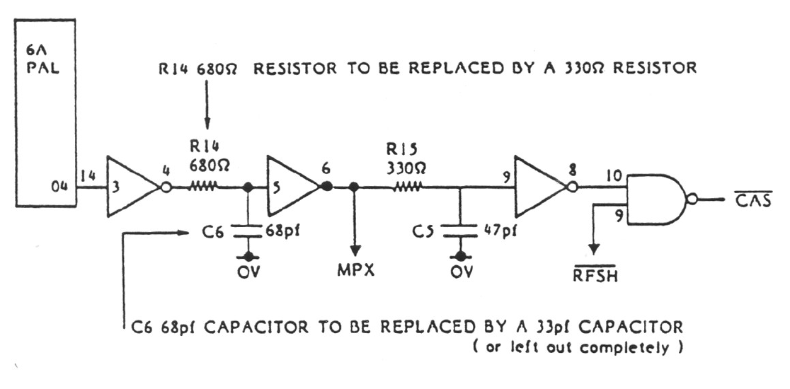
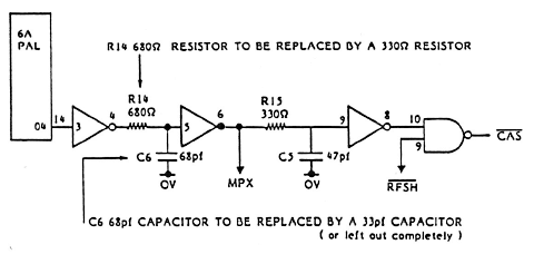
Note : The Service Manual describes
changes made to the Timing Chain from October 1984 to
resolve "occasional faults occurring after about 2 hours of
use - and poor fire up response. (especially when running in
conjunction with F.D.X.). The diagram below shows what
components were changed and to what values:-
R14 680 Ohm resistor to be replaced
by a 330 Ohm resistor.
C6 68pf capacitor to be replaced by a
33 pf capacitor (or left out completely).
Memotech noted that "You may
feel the need to replace the timing chain with the modified
circuit if your MTX is suffering from intermittent fire ups
(e.g. 1 fire up failure in less than 5 attempts constitutes
a possible fault in the timing chain circuitry). However,
the RAM logic description in these pages is based on the
original circuit design which will be found in machines
shipped before October 1984.
MTX DRAM
Operation <
Previous
Page Goto
Next
Page > ROM
Enable Signals
|