|
 |
The Memotech MTX Series
|
 |
MTX Series DRAM
Disclaimer
These pages were written as I attempted to gain a better
understanding of how the CPU and RAM interact in a Memotech
MTX series computer. The notes here are very much focused on
DRAM technology of the 1980s and some statements and "facts"
may not hold true for more modern implementations of DRAM.
The information here will likely evolve as I learn more, but
it is not guaranteed to be
accurate and may contain glaring errors, obvious to anyone
who knows about these things - if you spot any, please let
me know.
[ Skip the basics and
Goto Next
Page > Z80 Processor DRAM
Interface ]
DRAM - Overview
Dynamic RAM is based on a relatively simple design, only
requiring a single transistor and capacitor for each bit of
storage in the memory chip, the charged state of the
capacitor representing a logic "1" and the discharged state,
logic "0". As a result of this "simplicity", DRAM
has a higher density and is cheaper than static RAM (SRAM).
The penalty for this simplicity is related to the inherent
characteristics of the capacitors, whereby the charge gradually
dissipates, in the case of the microscopic capacitors in a
DRAM, the charge dissipates in a matter of milliseconds. In addition, the action of
just reading the state of
the stored bit also discharges the memory cell. To retain
the "memory", the charge must be periodically "refreshed",
the memory is therefore described as dynamic,
rather than static.
Some History to illustrate basic
principles . . .
Structure
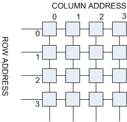
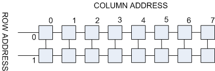
Some of the earliest DRAMs had a memory
capacity of only 1024 bits, they are referred to as 1k x
1-bit memories. The 1024 memory cells were arranged in a 32
x 32, two dimensional, square matrix as shown in the diagram
:-
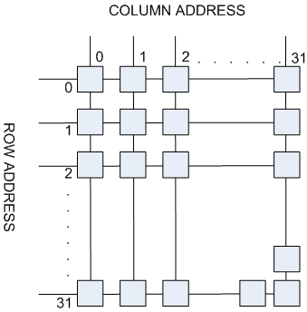
| In order to address each cell by its x and y
co-ordinates, external address lines needed to be able to
carry 32 unique row and column addresses, i.e.,
25 for each, requiring a total of 10
address lines. Including the power and control
signals (discussed later), it can be seen that
the footprint of the RAM was relatively large,
requiring a total of 16 pins to include all of
the required address lines for a 1024-bit
memory.
As memory sizes increased, this would have
become increasingly costly and/or impractical. |
 |
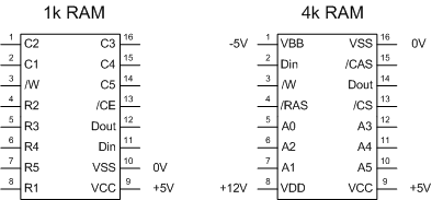
| To overcome this problem,
Mostek designed a method of multiplexing the
address lines so that the same pins on the chip
could transfer both the column and row addresses
from the bus to the RAM. These
footprints for 1k x 1-bit and 4k x 1-bit RAMs
demonstrate how the number of address lines has
been reduced and two additional signals added,
RAS
and CAS.
|
 |
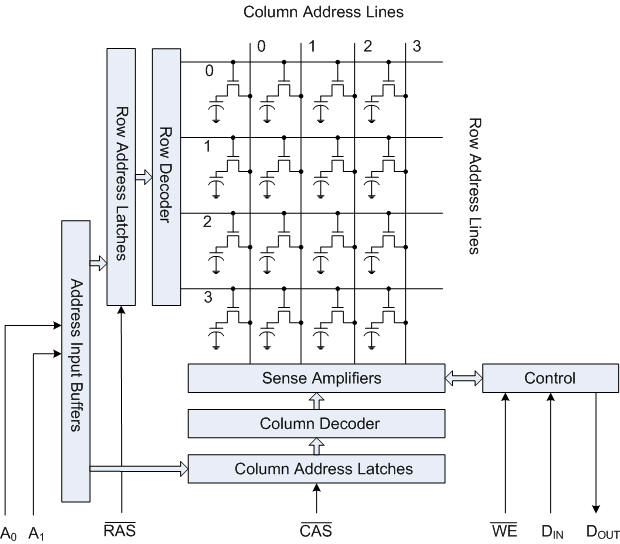
Addressing
Multiplexing of the address lines was a key milestone in
the development of DRAM. The number of address lines, and hence
the chip footprint, is reduced by multiplexing the row and
column address lines - the same address lines are used to
access the row and column addresses by setting them
separately using the Row Address Strobe (RAS)
and Column Address Strobe (CAS)
signals.
DRAM data sheets include timing diagrams for the various
modes of operation of the RAM such as Read, Write and
Refresh. A simplified diagram for a Read is shown here to
illustrate the principle :-
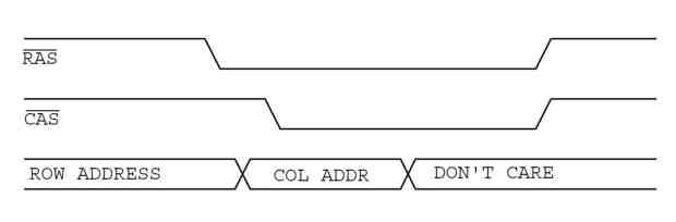
When a memory access is initiated for a Read or Write
operation, the memory controller first
puts the row address of the target memory cell on the
address bus and strobes the
RAS
signal low. The RAM latches this address and a short time
later, the memory controller puts the column address of the target memory cell on the address bus and strobes the
CAS
signal low while
RAS is still low.
Finally, the RAM decodes the Row and Column addresses to
identify the target memory cell.
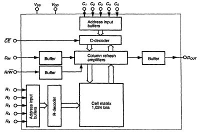
The RAM in Memotech MTX computers operates on this
principle, they are all 1-bit RAMs using
RAS /
CAS
multiplexing.
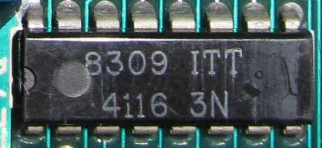
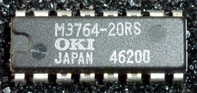
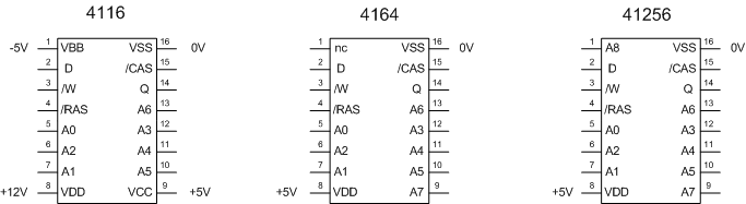
The Video RAM in all Memotech computers is ITT 4116,
the main memory in MTX500/512 and RS128 models is usually
the OKI version of the 4164
(with half working 64k RAMs in the MTX500) and the RAM in
the MTX512S2 are various supplier's versions of the
41256. As the diagrams show, the footprint of all of
these RAMs is the same, although the pin-outs vary as the
number of address lines increases and the voltage
requirements are different between the 4116
and the larger RAMs. As these are 1-bit memories, 8 of each
are required to provide storage for byte (8-bit) sized
storage.
|
16k x 1-bit Video RAM |
64k x 1-bit
Main Memory |
256k x 1-bit
Main Memory |
|
 |
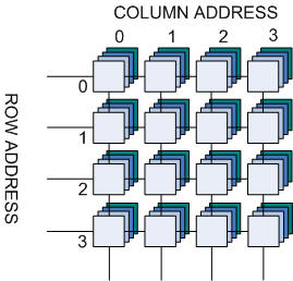
| Although not relevant to a
discussion Memotech MTX computers, higher
capacity DRAMs can be formed by creating a 3-dimensional
matrix as illustrated by the simple example of a 16 x 4-bit
memory structure (lower layer address lines omitted for
clarity) :- |
| |
|
|
|
|
|
16 x 1-bit |
16 x 4-bit |
Refresh
| Adding a little more detail to
the 16 x 1-bit
RAM above :-
Internal to the RAM, there would be 4 row
address lines and 4 column address lines, using
RAS /
CAS
multiplexing, this would require 2 external
address lines
As described earlier, the logical state
("1" or "0") of each memory cell depends on the
stored charge in capacitors and DRAMs need to have their memory
periodically refreshed on a frequent basis,
this only requires that power is applied to each row of
addresses in turn. |
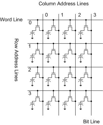 |
Using a technique called RAS Only
Refresh; the memory controller puts the required row
address on the address bus and strobes the RAS
signal low, the CAS
signal remains high and the RAM interprets this as an
instruction to refresh the memory cells on the row number
present on the address bus. This process is repeated for each
row under the direction of the memory controller. In the simplistic example above, to fully refresh the
memory, the 4 x 4 matrix would require 4 refresh operations,
a 64 x 1 bit memory arranged as an 8 x 8 matrix would
require 8 refresh operations and a 64k x 1 bit memory arranged
as a 256 x 256 matrix would require 256 refresh operations.
By rearranging the layout of the memory cells, refresh
operations can be significantly reduced, e.g., as
illustrated below, by just changing the matrix from 4 x 4 to
8 x 2, the number of required refresh operations is halved
for the same number of addresses.
Read / Write Operations
Adding, but not getting too deeply into, the additional
electronics required to Read and Write the memory cells,
That concludes my overview of DRAM basics, to see how DRAMs
work in a Z80 processor environment, see the
Next Page.
MTX Memory
Maps <
Previous
Page
Goto Next
Page > Z80 Processor DRAM
Interface
References used in creating the RAM pages on this site
Phoenix MTX Operators Manual
Memotech MTX500/512 Service Manual
The Memory section of Andy Key's
Memotech MTX Hardware page
Build Your Own Z80 by Steve Ciarcia
OKI Semiconductor
MSM3764
Datasheet
Georgia Tech
School of Electrical and Computer Engineering
Advanced Computer Architecture, ECE4100/6100,
Hsien-Hsin S. Lee
- Links to
Introduction to DRAM. Source:
Book Excerpt DRAM Circuit Design : A Tutorial,
from Wiley Publishers ISBN:0780360141
Tim Olmstead
|